20 Common Q&A About SMT Assembly
SMT assembly streamlines electronics manufacturing with compact, reliable designs using precise equipment, meeting high-density demands and international standards.
Surface Mount Technology, or SMT assembly has been one of the important bases of modern electronics manufacturing. These have enjoyed a wide range of advantages in the production of compact and reliable electronic products. To help you understand in detail the processes and applications of the SMT assembly, here are 20 commonly asked questions with detailed answers.
What is SMT Assembly?
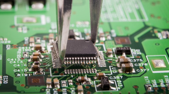
The SMT assembly, in contrast, involves mounting the electronic components on the surface of printed circuit boards. It involves the use of Surface Mount Components or Surface Mount Devices and will require specific assembly equipment to be able to provide functionality of compact and efficient designs effectively.
What Equipment does SMT Assembly Entail?
Key equipment for SMT assembly includes solder paste printer, chip mounter, reflow soldering oven, Automatic Optical Inspection systems, accessories, magnifying lenses/microscopes to perform special scrutiny. Note
What Are the Attributes of SMT Assembly?
SMT assembly, on other hand, prefers over THT due to its capability for higher assembly density, compactness, lightweight, and better reliability with fewer defect rates. It improves throughput and automation potential and reduces both EMI and RF interference.
How Does SMT Assembly Differ from THT Assembly?
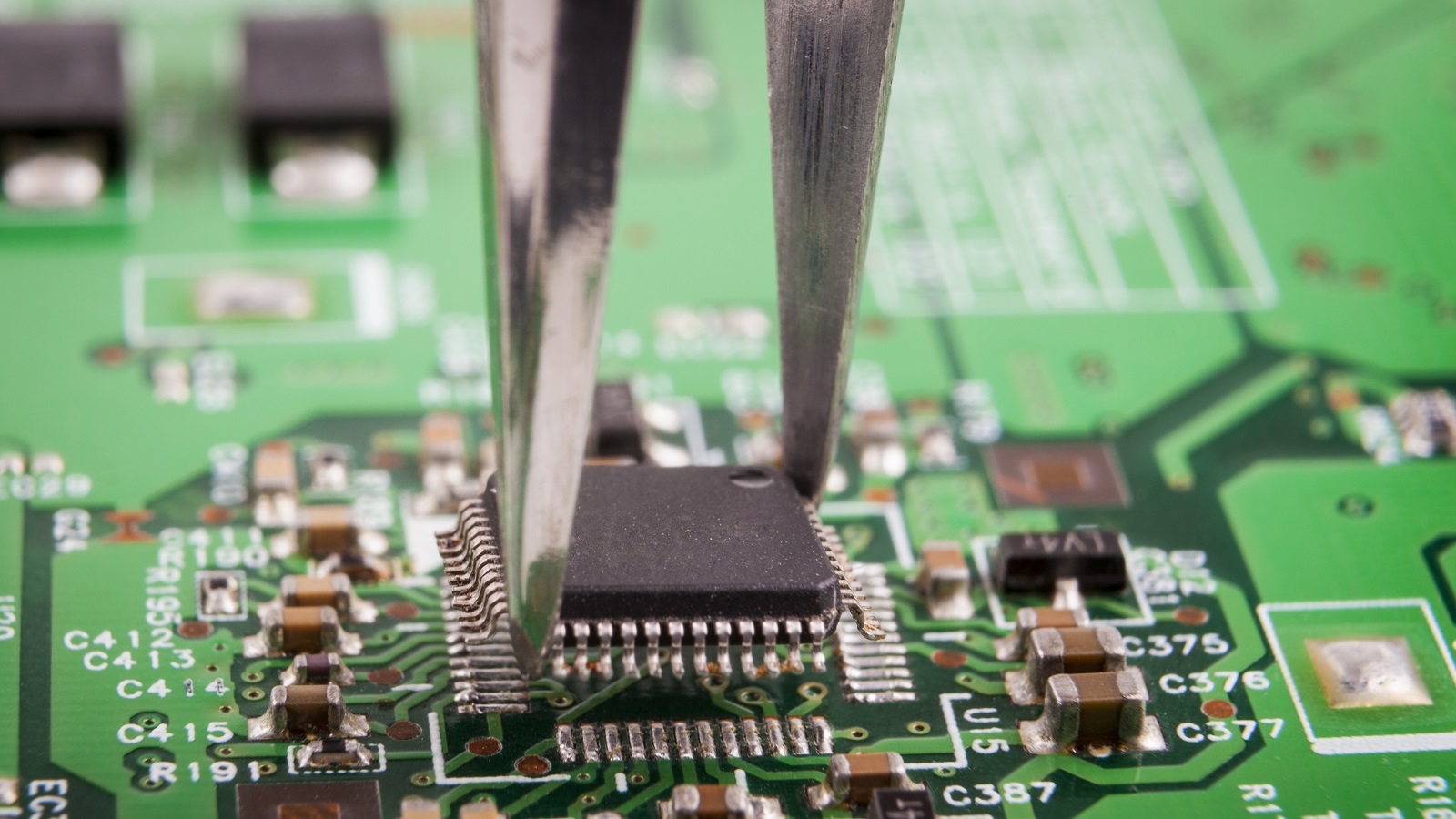
There are numerous vital differences among SMT assembly from THT: The SMT components do not have leads passing through the PCB as in THT. Another foremost advantage of SMT is that no holes have to be drilled, which is imperatively required in THT. In contrast to wave soldering in THT, reflow soldering is mostly utilized in SMT. SMT is highly automated, whereas THT relies primarily on human work. In SMT, components are often more lighter and much smaller.
Why Does Electronics Manufacturing Use SMT Assembly So Much?
SMT assembly meets the miniaturization and functional integration push of the electronics industry, thus becoming ideal for IC components of high density. It can respond to international standards in electronic manufacturing by meeting the needs of volume production, automation, and cost reduction.
Where Does SMT Assembly Get Used?
SMT assembly is used in sophisticated electronics, computers, telecommunications, automobiles, medical devices, industrial controls, military and space applications.
What is the General Manufacturing Process of SMT Assembly?
The general manufacturing process for SMT assembly includes solder paste printing, chip mounting, reflow soldering, and AOI. It may also include X-ray checks and some rework. For each process, a visual check would let one know if it has defects or not.
What is Solder Paste Printing and its Role in SMT Assembly?
It is among the processes that involve the application of solder paste via a stencil onto the PCB pads. It is one of the important steps in securing the component to the surface of the PCB before it undergoes reflow soldering.
Chip Mounting: What Is It and Its Purpose in SMT?
Chip mounting refers to placing the components onto solder-pasted pads on the PCB. In fact, it is a principal process in SMT assembly, that assures accuracy of the placed components and their temporary hold by the adhesive properties of the solder paste.
What Type of Soldering Is Used in SMT Assembly?
Reflow soldering is the industry standard for SMT assembly. A succession of regulated heating steps in a reflow oven hold the components in place. This allows the solder paste to melt and then solidify, permanently holding the components in place.
Do PCBs Need Cleaning After SMT Assembly?
Yes, there does exist a serious need for cleaning PCBs after SMT assembly because of solder residues, flux, and contaminants. That is one of the most important steps within product reliability and performance.
What Kind of Inspection Is Used by SMT Assembly?
PCB quality may be ensured using a variety of inspection methods, including AOI for finer details, X-ray inspections for concealed solder connection flaws, and basic visual inspections that can identify obvious problems.
What Requirements Must an SMT Assembly Workshop Meet?
The surroundings of a workshop should be controlled, for instance temperature at 25±3°C with humidity 45% to 75% RH, height of the ceiling 3 meters with good static grounding with an electrostatic discharge guideline of 150KR±10%.
What is the Role of Flux in SMT Assembly?
It plays a very important role in the reduction of oxidation, and it enhances solder wetting. The result of such an action will be good solder joints after the reflow process.
How Does a Pick-and-Place Machine Work?
The Pick-and-place machines are the automated machines which place components based on their pre-programmed instructions; it collates the component onto the PCB with speed and accuracy at high turns of speed.
How Does Automated Optical Inspection Work?
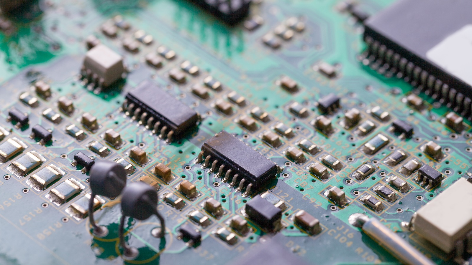
AOI deploys cameras combined with software algorithms that actually carry out the inspection of the PCBs for defects, such as misplaced components or improper solder joints, among others.
With the Miniaturization of Components, What Is the Impact on SMT Assembly?
With such miniaturization, assembling and placing ever-smaller components requires a precision that is correspondingly high; hence, it raises the demand for high-end equipment and cautious process control even further.
What are Common Defects in SMT Assembly?
The defects vary from component misalignment through solder bridges, tombstoning, or poorly wetted solder joints.
What Should be Considered in SMT Design?
Good SMT design requires consideration of pad size and geometry, spacing between components, thermal management issues and layout for best performance during the process of assembly.
How Has SMT Assembly Evolved Over Time?
With miniaturization and automation coming into demand, the SMT assembly had to improve with better material, equipment, and process.These new improvements in SMT materials, equipment, and processes build advanced electronics with more sophisticated and high-density circuits.
At PCBX, we specialize in providing premium PCB solutions that are fully capable of meeting the new demands placed on SMT assembly, which is for the excellence in electronics manufacturing.
Hot Tags:
Contact us

If you can't find what you're looking for, please contact us.
Article
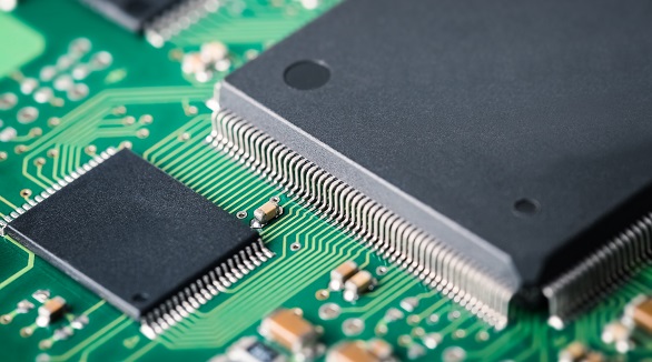
Surface Mount Technology (SMT) revolutionized electronics, facilitating smaller, faster, and more reliable products. It mounts components directly on PCBs, enabling miniaturization and automation. Though SMT boosts space efficiency, cost-effectiveness, and reliability, it poses rework challenges and requires high initial investment.
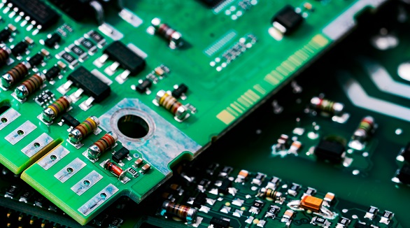
Printed Circuit Board Assembly (PCBA) employs Through-Hole Technology (THT) and Surface Mount Technology (SMT). THT offers robust mechanical bonds, ideal for high-stress applications, whereas SMT supports efficient, high-density assemblies. Each method has unique advantages and limitations, impacting cost, manufacturing efficiency, and component compatibility. Understanding these differences is key for optimal PCB design.
Still, SMT can further feature defects such as solder bridging, cold solder joints, tombstoning, and solder balling. Grasping the very common faults and their solutions is the key toward effective PCB assembly and reducing SMT errors—very much in line with the trend toward PCB miniaturization and higher component density.
