3-Layer PCBs
3-layer PCBs offer a balance of cost and complexity with benefits like improved signal integrity, reduced EMI, and increased component density for varied applications.
In the complex electronic world, a Printed Circuit Board (PCB) is the platform for innovation on which electronic components are mounted in a structured format and interconnected. While single-layer and double-layer PCBs have been sufficient to meet the simple applications, more complicated electronics require further advanced designs. The 3-layer PCB finds its place as the middle ground for balancing functionality and cost-effectiveness.
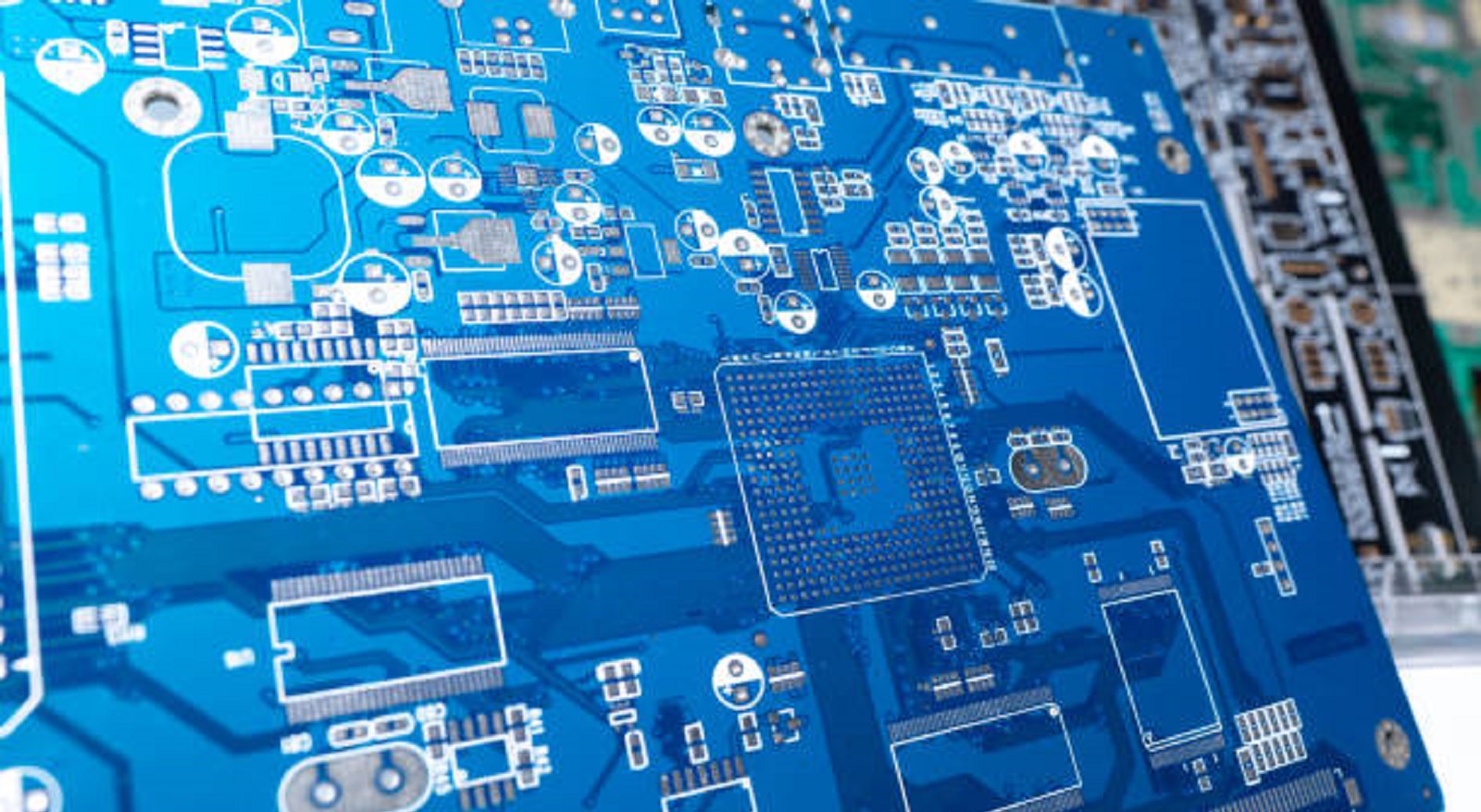
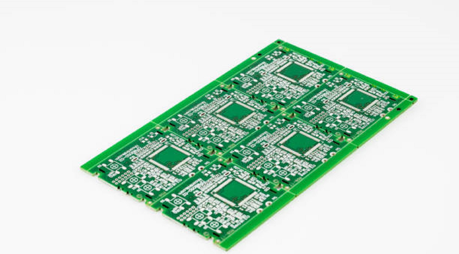
A 3-layer PCB consists of three conductive layers separated by insulating substrates. Although less common than their multi-layer counterparts—such as 4, 6, or even 32-layer boards—the specialized design of 3-layer PCBs offers unique advantages for specific applications. RayMing, a notable manufacturer of 3-layer PCBs, highlights their potential in scenarios requiring specialized performance without escalating costs. Whether driven by unique design demands or cost-saving objectives, 3-layer PCBs provide an alternate path for bridging the gap between complexity levels.

Advantages of 3-Layer PCBs
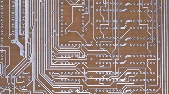
Increased Routing Flexibility: The added layering allows for increased complexity in routing, which is beneficial for increased connectivity and better circuit optimization. This is particularly relevant in applications that include space constraints or complexity in design where using a simpler board would not be adequate.
Improved Signal Integrity: A continuous ground plane at the middle layer can provide controlled impedance and reduced interference for better signal integrity in high-speed or sensitive applications.
Reduced EMI and Noise: Signals between power and ground layers reduce electromagnetic interference (EMI) and cross-talk, thus cleaner signal pathways.
Better Power Distribution: The extra layer will allow for efficient pairing of power-ground planes, which can improve power distribution across different voltage domains.
Increased Component Density: Using both sides for SMT component placement will allow for denser board designs while supporting higher component density.
Versatile Mixed Signal Designs: 3-layer boards facilitate the segregation of analog and digital signals, accommodating mixed-signal designs more efficiently.
These advantages make 3-layer PCBs an excellent choice for balancing performance and cost in numerous applications.
Construction of 3-Layer PCBs
The fabrication of 3-layer PCBs involves laminating three copper layers with insulating dielectric substrates, primarily glass-reinforced FR-4. Key construction steps include:
Core Substrate: It forms the mechanical back-bone upon which the whole assembly is based.
Lamination: The board's conducting surfaces are laminated copper foils over the core.
Photo Lithographic Processing: In this process, specific circuit traces, pads, and features are produced by patterning the copper layers.
Via and Hole Fabrication: Plated-through holes and vias enable electrical connections to be made between vertically stacked layers.
Soldermask Application: Protective soldermask isolation and shielding for the copper traces.
This sequence of process is critical in manufacturing 3-layer PCBs. It provides a more refined base for the mounting of components.
Common 3-Layer PCB Stackups
Flexibility in design makes it possible for 3-layer PCBs to have many configurations. These configurations are based on performance requirements as follows:
Ground Plane Configuration: The central layer has a ground plane between outer layers, enhancing controlled impedance and shielding.
Split Power Planes: The split power planes allow isolated power supply domains within the central layer for VCC and VDD.
Buried Signal Plane: Features a middle plane dedicated to signals, encapsulated by ground layers, enhancing isolation and signal purity.
These configurations, modifiable based on thermal, EMI, and isolation needs, make 3-layer PCBs adaptable to diverse requirements.
Design Considerations for 3-Layer PCBs
Effective utilization of 3-layer PCBs requires meticulous attention to design specifics:
Power Plane Management: Proper splitting of power planes is crucial for optimal performance in digital and analog domains.
Signal Layer Optimization: Critical signals should be placed and routed in the outer layer near power/ground planes strategically.
Via: High-density via stitching helps to reduce impedance problems, providing better connectivity efficiency.
Thermal Management: Maximizing copper areas on outer layers enhances heating capabilities.
Signal Integrity Simulation: In detail, with a signiffic representation of power and ground impedances can ensure more suitable robust designs that eliminate resonance and emission issues.
These factors direct engineers to refine their 3-layer PCB designs for reliability and performance.
Applications for 3-Layer PCBs
3-layer PCBs find general use in a wide range of applications within different industries:
Consumer Electronics: IoT-enabled devices, home automation appliances, and wearables require PCBs with fewer layers but perform complex functions.
Automotive Electronics: Infotainment modules and GPS modules require a trade-off between the size and functionality that is addressed by 3-layer PCBs.
Industrial Controls: PLCs and motor controllers rely on 3-layer structures for reliable operating performance.
Medical Devices: Diagnostic and monitoring instrumentation take advantage of the reliability of 3-layer PCBs to support critical function.
The wide range of applications demonstrate the widespread application of 3-layer PCBs in contemporary electronic design.
3-Layer PCB Fabrication
3-layer PCBs are fabricated using a number of detailed manufacturing processes:
Material Selection: Core substrates and copper foils are chosen according to design requirements.
Imaging and Patterning: Advanced imaging processes, including photoresist application and laser patterning, determine the circuit pattern.
Layer Lamination: High pressure lamination of the layers makes the structure very rigid.
Drilling and Plating: Precise drilling followed by copper plating creates strong electrical connections.
Testing and Assembly: Thorough testing is done before component assembly in order to provide board quality as well as performance.
High yield fabrication processes are the foundation for cost-effective large-scale production of 3-layer PCBs.

The 3-layer PCBs combine the greatest amount of complexity with cost-effectiveness in PCB design, and it addresses a wide range of electronic application requirements. As technology continues to push its demand upward, more significant roles for 3-layer PCBs are placed in the bridging link between traditional designs and more complex multi-layer solutions. As materials and manufacturing evolve, 3-layer PCBs promise to offer better performance, reliability, and cost savings in industrial and consumer electronics. Given that PCBX is committed to leading the PCB technology revolution, we stand at the forefront of its evolutionary path, which unlocks the full capability of a 3-layer configuration for designers.
Hot Tags:
Contact us

If you can't find what you're looking for, please contact us.
Article

10 oz copper PCBs offer high current capacity, improved thermal management, and durability for demanding applications in power electronics, aerospace, and military.

Select aluminum PCBs for excellent heat management or FR4 PCBs for cost-effective versatility in diverse electronic applications.

Black FR4 PCBs offer aesthetic and functional benefits, including light blocking, heat dissipation, and enhanced signal performance, suitable for electronics.
