- Products & Capabilities

- About
- Resources
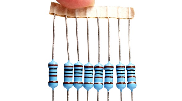
8 Common Errors in Surface Mount Technology (SMT)


Still, SMT can further feature defects such as solder bridging, cold solder joints, tombstoning, and solder balling. Grasping the very common faults and their solutions is the key toward effective PCB assembly and reducing SMT errors—very much in line with the trend toward PCB miniaturization and higher component density.
Surface mount technology does not guarantee zero-defect soldering. Typical surface mount technology faults that can lead to PCB failure will be discussed in this article, along with strategies to reduce the risk. For PCB assembly services to be provided effectively, this is crucial.
It is necessary, however, before discussing the common defects in SMT assembly, to gain insight into the basics of SMT:
What is Surface Mount Technology?
Surface mount technology, or SMT, is a process for mounting electronic components directly onto the surface of a printed circuit board (PCB). The components mounted in this way are called surface-mount devices (SMDs).
What are the Advantages of Surface Mount Technology?
SMT offers several advantages over through-hole mounting, such as facilitating automation and allowing for larger component densities on the PCB. Further, SMT can realize faster circuit speeds and improve high-frequency performance.
What is the Difference Between Through-Hole and Surface Mount Technology?
Several differences exist between surface-mount and through-hole technologies. The major ones include cost, automation, board space, and component density. On the aspect of cost, through-hole components are generally more expensive to make as opposed to SMT parts. Coupled with that, they can't be used for automation. Compared based on board space and component density, through-hole technology is always at a limit compared to SMT.
Surface Mount Technology Troubleshooting
SMT Error #1: Solder Bridging or Electrical Bridging
Solder bridging occurs when the solder enrolls between two conductors that otherwise are electrically isolated, leading to electrical shorts and malfunction of circuits.
Possible Causes:
Solder Paste Printing Issues: One of the most common causes of bridging is misalignment within the solder paste printing process. Misalignment may be from an incorrect alignment of the print or the stencil concerning the pad layout on the PCB.
Excess Deposition of Solder Paste: Too much solder paste can cause bridging. This situation mostly occurs when the stencil aperture-to-pad ratio is too high.
Solder Paste Cold Slump: This could be another cause of the occurrence of bridging. The wrong solder paste metal-to-flux weight ratio may be the culprit. High temperatures and high humidity further exaggerate the problem.
Reflow Profile Inadequacies: The reflow process intends to melt solder paste powder particles, and wet surfaces to be joined, and solidify the solder to form a metallurgical bond. There are four zones in the reflow profile: preheat, soak, reflow, and cool-down. If the preheat zone has a slow ramp rate, this may result in bridging. If the soak has a long time duration, this can result in a paste hot slump, which can contribute to bridging.
Placement Inaccuracy: Incorrect placement can reduce the distance between pads, making it easier for bridging to occur. Pressure applied during component placement may also squeeze solder paste from the pads.
Possible Solutions:
Use the Right Solder Paste Metal-to-Flux Weight Ratio: Ensure that there is no solder-paste slump. For instance, typical dispensable solder paste has 85-87% metal content, which would slump in fine-pitch SMT printing. Consider a ratio closer to 90% metal for stencil-printing applications.
Use a Proper Reflow Profile: Develop a proper reflow profile to ensure neither cold nor hot solder paste slump.
Appropriate Alignment of Stencil-to-Pad: Automatic printer alignment systems shall be employed to ensure proper alignment of stencil apertures relative to the pads.
Component Placement Accuracy: The components shall be precisely placed under the correct pressure so that all the solder paste will not be squeezed out of the pad.
Edit Stencil Aperture Size: Reduce the stencil aperture dimensions by 10% or reduce the stencil thickness to deposit lesser solder paste.
SMT Error #2: Inadequate Solder Joints or Electrical Opens
Electrical opens occur when two electrically connected points to one another are separated and hence interrupt the designed circuitry. This causes malfunctioning circuits.
Possible Causes:
Solder Paste Printing Problems: This defect mainly emanates from the solder paste printing stage. Insufficient solder on the joint may cause an open circuit. It normally occurs due to solder paste clogging the apertures of a stencil.
Coplanarity Issues: Even with the correct solder volume, an open may still occur due to a non-contact condition between the solder and the lead or pad during reflow. It is a condition called component lead coplanarity.
PCB Fabrication Flaws: Opens can also result from problems in the fabrication of the printed circuit board.
Possible Solutions:
Aspect Ratio Optimising: The aspect ratio is the relationship between the width of the aperture to the thickness of the stencil. This should be optimized since a very small aspect ratio may be indicative of the clogging of solder paste in the apertures.
Control of the Environmental Conditions: This should be rigidly avoided since extreme conditions should not prevail in the manufacturing process. Other than this, controlled conditions also make sure that there won't be any contamination of the solder paste in case a clean environment is maintained.
Coplanarity Investigation: Ensure that coplanarity issues are investigated and proper action is taken to ensure that the handling of electrical opens is done.
Quality of Fabrication: Check out the quality of the fabrication process with the PCB supplier.
SMT Error #3: Solder Balling
Solder balling occurs when small balls break off from the rest of the sphere of the solder. These little balls can easily create functional failure in the circuit because they tend to bridge across adjacent leads carrying undesired current. Of course, this problem is especially pernicious in no-clean processes because the solder balls are not washed away.
Possible Causes:
Moisture Contamination: Moisture contamination of solder paste is the major cause of solder balling. It leaves behind a solder sphere while soaking in reflow.
Faulty Reflow Profile: Faulty reflow profile mainly at times when the preheating rate is too high and does not give room for gradual evaporation of solvents, hence forming solder balls.
Oxidation: Excessive oxide on the solder powder in the paste can also be the cause of solder ball formation.
Solder Paste Printing Defects: Misregistration during solder paste printing puts the paste on the solder mask instead of the pad. These misregistered solder pastes are responsible for solder balling.
Smeared Solder Paste: While printing, the paste smears onto the bottom side of the stencil, adding to this problem as well.
Possible Solutions:
Coarser Powder Use: Fine powder size tends to have more oxides and is more prone to slumping. This can be somewhat mitigated by using coarser powder.
Optimization of the Reflow Process: Proper design of the reflow process with evaporation/reflow to suit the solder paste in use.
Moisture and Humidity Control: Avoid the reaction of solder paste with moisture and humidity, which could cause contamination.
Minimum Print Pressure: A minimum required print pressure must be put on the stencil at all times so that there aren't any smearing effects.
Check Regularly for Print Alignment: The print alignment must be checked before parts are reflowed into place.
Cleaning the Stencil Regularly: The bottom side of the stencil has to be cleaned regularly to avoid any smearing effects.
SMT Error #4: Tombstoning
Tombstoning is the condition where a chip component partially or wholly lifts off the pad, placed vertically with only one end soldered. This happens due to the imbalance in forces during the reflow soldering process that results in open circuits.
Possible Causes:
Differential Heating: The heating across the terminals of a component may occur at differentials, so reflowing takes place at one end before the other and raises the other end of the component, effectively doing so.
Differential Heat Sinks: The ground planes inside the layers of a PCB can work like heat sinks and may draw heat away from the pad, which might further drive in imbalanced heating.
Environmental Exposure: Temperature and humidity can lessen some of the force of solder paste. This may be responsible for the movement of components out of position during reflow.
Excessive Movement: Excessive movement during and after reflow might misplace the component, resulting in tombstoning.
Unequal Placing of Component: The poor placement of a component on pads initially can cause an imbalance in the force given by the solders.
Possible Solutions:
Ensure Coverage: The body of the component shall cover at least 50% of both pads to prevent an imbalance of the solder forces.
High Accuracy of Component Placement: The accuracy of placing the components is very high.
Preheat Temperature Should be High: The temperature in preheat has to be kept high so that during reflow, at its ends, there will be less differential heating.
Less Movement: Less movement is required in SMT assembly and reflow.
Low Environmental Exposure: The exposure to temperature and humidity should be at the very minimum because, as is well known, it reduces the strength of solder paste.
Longer Soak Zone: A longer soak zone in the reflow profile allows the wetting forces to be flattened on both pads before they get into their molten state.
SMT Error #5: Non-Wetting or De-Wetting
Non-wetting or de-wetting is a situation where the fluid solder fails to wet one or more components. Its effect is to leave areas on the surfaces in contact with liquid solder without adhesion.
Possible Causes:
Poor PCB Finish: Visible base metal, which is harder to solder to, can cause non-wetting.
Over Soaking Time: If soak time during reflow is too long, flux may be spent before reaching the temperature for soldering and thus will not wet.
Insufficient Heat: In the process of reflow, in case of too little heat, flux does not attain its temperature of activation, and this leads to non-wetting.
Possible Solutions:
Improve Metal Surface Finish: Use high temperature-resistant OSP or ENIG finishes.
Avoid Excessive Profiling Time: Reduce the time spent profiling before entering the reflow stage.
Use the Right Flux: Use the appropriate flux for a soldering job.
SMT Error #6: Solder Beading
Solder beading refers to a condition wherein bigger solder balls are created around discrete components placed too close to each other, which may cause functional problems like solder balling; however, these beads stick only to discrete components.
Possible Causes:
Too Much Solder Paste: This is usually due to excess deposition of solder paste.
Flux Outgassing: The outgas flux at preheating may overcome the coalescence force of the paste to form solder beading.
Excessive Placement Pressure: If the pressure of component placement is too great, it forces out the solder paste onto the solder mask and doesn't fuse back into the joint.
Possible Solutions:
Thinner Stencil: Or reduce aperture dimensions by about 10% to address the side where the solder bead occurs.
Less Placement Pressure: Apply reduced pressure during the pick and place operation of the component.
SMT Error #7: Inadequate Fills and Insufficient Solder
This fault occurs due to an insufficient quantity of solder paste dispensed relative to the dimensioning of the stencil opening aperture. There isn't enough solder for a proper fillet to form at the component leads after reflow.
Possible Causes:
Clogged Stencil Apertures: Dried-up paste blocks the stencil aperture.
Insufficient or Excessive Squeegee Pressure: Either too high or low pressure during the print cycle will allow inconsistent quality in the deposition of solder.
High Squeegee Speed: If the squeegee speed is too high, there is little time for the solder paste to roll into the apertures and onto the pads.
Too Low a Viscosity or Low Metal Content in Solder Paste: If the solder paste is too thin or the metal content is lower than specified, then insufficient fills may take place.
Possible Solutions:
Segment Large Openings: Segmented large apertures avoid excessive squeegee pressure.
Clean Stencil Regularly: Clean the stencil regularly; check the paste for expiry/dryness. Good board support should be provided.
Squeegee Speed Control: Squeegee speed should be appropriate to ensure proper deposition of the paste.
SMT Error #8: Cold Solder Joint or Grainy Joint
Cold solder joints display poor wetting; they shall have a greyish appearance, porous, displaying dark, rough, non-reflective surfaces where they should be bright and shiny.
Possible Causes:
Insufficient Heat: The solder absorbs insufficient heat while being reflowed.
Too Little Flux: This could be a result of inefficient cleaning of components or PCB pads before soldering or there is too much impurity in the solder solution.
Possible Solutions:
Reflow Temperature Higher: The maximum reflow temperature should be such that it can melt the solder material completely.
No Movement: During or after the reflowing process, no motion should take place.
Alloy Analysis: Check for contaminant presence within the alloy analysis.
The challenges for PCB manufacturing are increased by the tendency toward miniaturization of the circuit boards. There is an increasing demand for more strictly controlled soldering procedures in line with the trend of PCBs incorporating smaller components. Reducing these frequent SMT mistakes increases the productivity of SMT manufacturing and provides more effective PCB assembly services.
Hot Tags:

Contact us

If you can't find what you're looking for, please contact us.
Article
Customers prefer one-stop PCBA service not only because of price transparency; it can save time and reduce labor costs with efficiency and professionalism in procurement and production.
 2024/07/29
Compared to THT, SMT offers better miniaturization and weight reduction in any electronic application. With the use of BGA packages, high-assembly density, reliability, and improved performance are achieved; on the other hand, this requires a rework and inspection that is not really common. PCBX specializes in the area of advanced SMT and BGA assembly to help drive modern requirements of compact electronic devices.
2024/07/26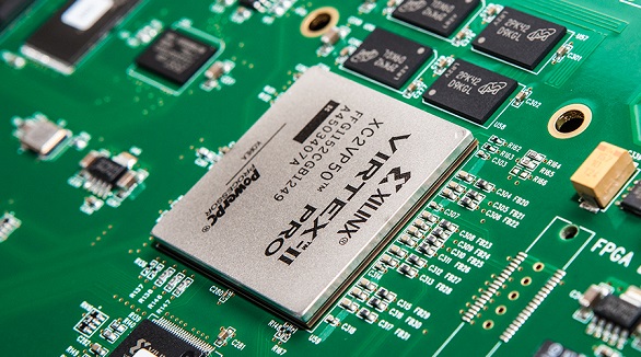
Ball Grid Array (BGA) components, such as PBGA, CBGA, CCGA, TBGA, and CSP, provide high I/O density, improved reliability, and high-quality electrical and thermal performance. Quality assembly and functionality are assured since advanced soldering and inspection methods are required, like AXI and AOI. Proper storage and handling shall guarantee the performance of the devices.
2024/07/26