Advantages and Disadvantages of SMT Assembly
Surface Mount Technology revolutionizes electronics, offering size, cost, and performance benefits, but poses challenges with high setup costs and handling.
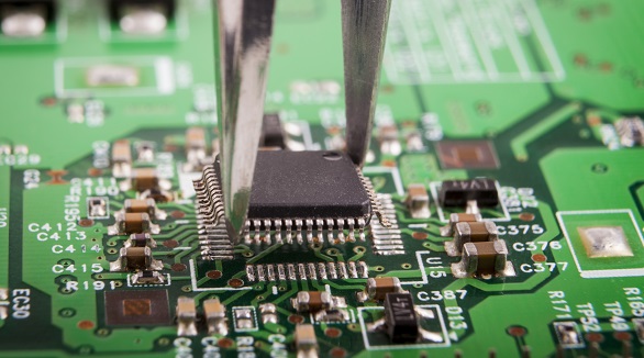
Surface Mount Technology has been considered among the most important technologies available nowadays for the assembling of modern electronic devices. It allows components to be mounted directly onto the surface of the printed circuit board and thus practically replaced the older technology called through-hole technology. Modern electronic devices, which are manufactured using this technology, have been called surface mount devices and revolutionized the design and manufacturing process of electronic circuits. The key advantages and disadvantages of SMT are discussed here in relation to the ongoing debate of SMT versus SMD and what this means for those either working with surface mount device distributors or designing surface mount PCBs.
Advantages
Weight and miniaturization
It has been one of the major driving forces for the adoption of SMT due to its assistance for the issue of considerable downsizing. Generally, SMT components are 60–90% smaller and lighter compared to through-hole components. This decrease in size especially affects product categories, such as consumer electronics, where goods have to be more portable and streamlined.
More Flexibility in PCB Design
The surface-mount PCBs can be constructed with more flexibility because an engineer might use both sides for mounting. This would necessarily mean that an application can be made full use of, all the space available, including providing complex circuit designs, including multi-layered ones. The SMT is one technology needed for functioning flex and rigid-flex PCBs, which allow advanced end electronics to combine resiliency and adaptability with compact design.
High-Speed Signal Transmission
Of all the technical benefits of SMT, its impact on signal transmission speed and quality is the most notable. Smaller lead lengths used in SMT design lower parasitic capacitance and inductance, enhancing signal integrity and speeding up transmission. SMT-assembled PCBs are also very suitable for high-frequency applications due to reduced radio frequency interference.
Automation and Manufacturing Efficiency
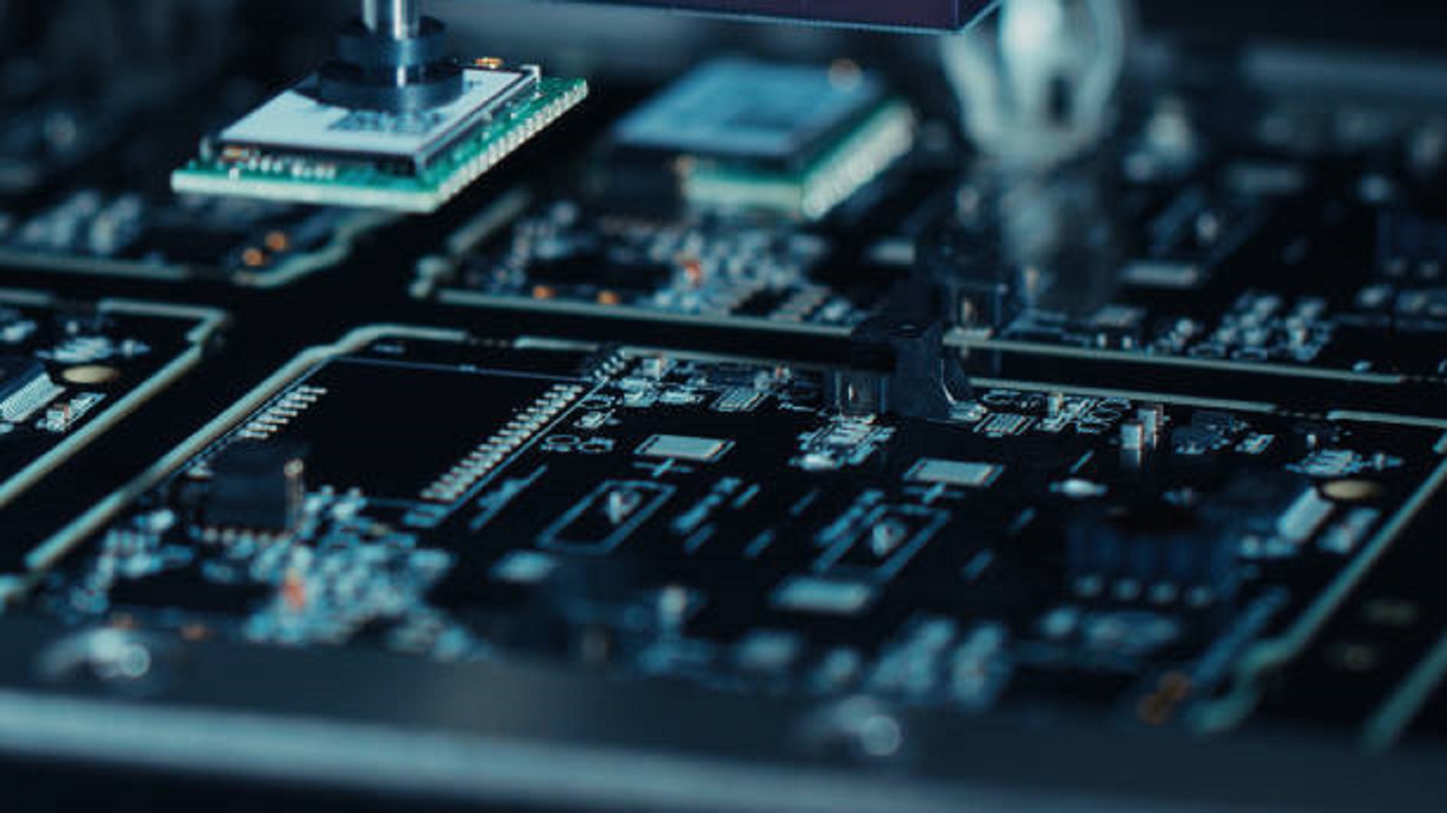
Because SMT allows automation, which greatly reduces production costs, automation is particularly suited for SMT. Compared with a person, the automated pick-and-place devices can insert components onto a PCB much faster and more accurately; hence, increasing production while keeping high quality constantly. This automation is imperative during large-scale production since, in most cases, the use of manual methods is utterly impossible.
Cost-Effectiveness
The cost of setting up SMT is very high initially, whereas the technology has long-term cost-effectiveness quite substantial. Smaller size of SMDs along with automation allows for a huge reduction of material handling, packaging, and shipping.Furthermore, the overall cost of materials is decreased because to the smaller area that SMT components occupy on the PCB.
Disadvantages
High Initial Equipment Cost
The high upfront investment required to establish an SMT line, including investments in pick-and-place equipment, reflow ovens, and highly advanced inspection systems, is undeniably the major barrier to entry for smaller companies. These up-front capital investments do appear daunting; however, they are crucial in allowing full exploitation of the benefits of SMT.
Complex Inspection and Repair
The component to be inspected and repaired-the SMD-is relatively smaller in size and more complex. For instance, solder joints on complex components like BGAs are hidden under the component. This makes conducting any sort of visual inspection rather challenging, and just to confirm whether the joints are intact, expensive, special equipment is needed.
Susceptibility and Handling Issues
Unlike through-hole components, SMDs are susceptible to both mechanical stress and ESD. As such, they can lead to debilitating damage if not handled properly, and they also have to be assembled in a controlled environment based on conditions that concern ESD protection. Because they are so sensitive, these elements have to be placed with care and precision, using special instruments and methods.
Not All Components Can Use This Technology
Though SMT supports a large variety of components, SMT does not support all types of components. High-power elements, such as large transformers, or heat-dissipation elements, like some power semiconductors, could not usually use SMT. In such cases, which are very common, SMT and through-hole components might be applied on the same PCB for different needs of application.
High Cost for Small Batch Production
Prototypes and small batches are disproportionately expensive to manufacture with SMT. Due to the initial cost of setting up the production line and the technical know-how required, which may be challenging for certain startups or small-scale firms, small-batch production is less cost-effective than large-scale manufacturing.
SMT vs. SMD
Despite their frequent interchangeability, SMT and SMD really relate to two distinct elements of electronic assembly. SMD is the component that is really being mounted using the technology, whereas SMT is the method or procedure for mounting components. This decision between using SMD within an SMT framework or sticking with through-hole technology in large measure is driven by particular needs for any given project in size, complexity, and volume of production.
These subtleties are very important to understand for the people involved either with a surface mount device distributor or in the fabrication of a surface mount PCB, as the optimization of product design and manufacturing processes involves these factors. The advantages of SMT in size reduction, production efficiency, and performance are offset by disadvantages of high initial costs and handling complexities.
In summary, Surface Mount Technology is a revolutionizing turn in the field of electronics manufacturing and thus predetermined the course of modern electronic development. While it offers great advantages with respect to size, cost, and performance, the constraints imposed on equipment costs and handling precision are major factors to be considered. As the industry moves further, this aspect will play a vital role in understanding these factors for the fullest utilization of SMT in many fields.
Hot Tags:
Contact us

If you can't find what you're looking for, please contact us.
Article
As PCB lines and components shrink, traditional visual inspection fails; AOI using DRC and CAD methods is crucial for quality SMT assembly, offering intelligent, accurate inspections.
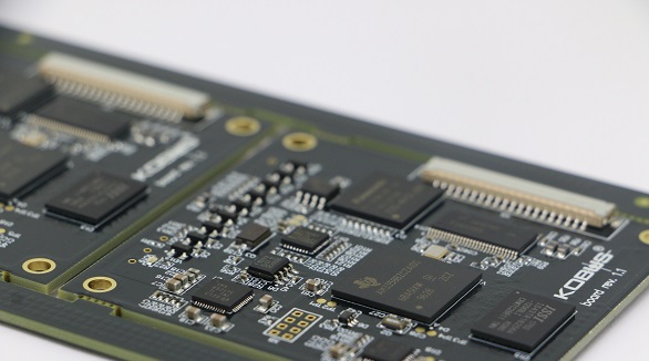
SMT assembly places components directly on PCBs, enhancing miniaturization, performance, and efficiency. Key steps: solder paste printing, chip mounting, reflow soldering, and inspection.
Still, SMT can further feature defects such as solder bridging, cold solder joints, tombstoning, and solder balling. Grasping the very common faults and their solutions is the key toward effective PCB assembly and reducing SMT errors—very much in line with the trend toward PCB miniaturization and higher component density.