- Products & Capabilities

- Simulation Design & EDA

- About
- Resources
Annular Ring Via in PCB


Annular rings are crucial for reliable PCB electrical connections. Proper sizing, understanding issues like tangency and breakout, and best practices ensure optimal performance and reliability in electronic circuits.
Printed Circuit Boards are the backbone of all modern electronic systems and provide the necessary electrical connections between diverse components. One of the important features in the design of a PCB is an annular ring. The effective design and manufacturing of annular rings assure reliable electrical connections. Overview This article will provide an overview of annular ring via through its importance, how to calculate its size, common issues, and best practices for optimum annular ring via performance.
What is an Annular Ring?
An annular ring refers to a ring of copper pad around a via or drilled hole on a printed circuit board. It looks much like a doughnut. This is where the different layers of the board will connect and, thus, is very important in the continuance of electricity. The middle hole would be where you insert wires or component pins, and once soldered, the annular ring gives a very stable and reliable electrical connection.
The Importance of Annular Ring Size
The size of the annular ring is important to ensure effective and reliable electrical connections. The width of the annular ring must be sufficient to accommodate manufacturing tolerances and avoid problems such as pad breakout that can reduce current-carrying capacity and affect overall functionality of the circuit. Normally, the minimum width of the annular ring should be greater than or equal to the design width specified in the design.
Calculation of Annular Ring Size
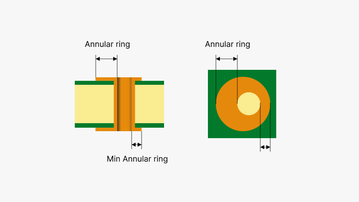
Mathematically, annular ring size can be computed as a difference between the diameter of the pad and the diameter of the hole, then divided by two. Assuming the hole diameter is 10 mils and the pad diameter is 24 mils, the annular ring width is calculated as (24-10)/2, amounting to 7 mils.
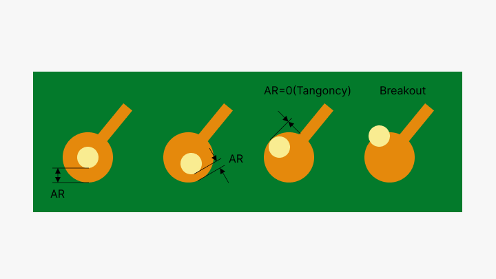
Common Issues with Annular Ring Vias
Despite of their importance, annular rings have a number of problems during the process of manufacturing on a PCB:
Tangency and Breakouts
Good Via: This is when the drilled hole is perfectly centered within the pad to make a uniform annular ring.
Tangency: This is when the drilled hole is off-center a bit, which makes its edge touch the edge of the pad.
Breakout: When the drilled hole is significantly off-center, placing it partially or completely outside the pad area.
Neither tangency nor breakout is preferable because it can affect the electric connection and general reliability of the PCB.
Annular Ring Issues
Manufacturing tolerances have a significant effect on the accuracy of the annular rings. Most PCB manufacturers, such as PCBX, have manufactured specified tolerances, which generally tend to be around 5 mils, within which the drilled holes could slightly be off their intended positions. In order to minimize risks, one may give additional space in cases beyond that of the manufacturer's tolerance.
One effective way of achieving this is by enhancing the annular ring size at least 1 mil more than the minimum specified by the manufacturer. This little margin allows for any change and makes provision for the electrical connections to be valid.
Considerations in Designing Annular Rings
Classifications in the Design of PCB
Depending on the PCB application field, the size of annular rings can be different. According to IPC, there are three classes of different printed circuit boards for their target applications:
Class 1: General Electronic Products
Class 2: Dedicated Service Electronic Products
Class 3: High-Reliability Electronic Products
Consequently, PCBs made for high-stress applications-like Class 3-larger annular rings are required.
Getting the Size of the Annular Ring Right
To get the annular ring size right, consider the following suggestions:
Leave Enough Clearance: The width of the annular ring should be large enough to accommodate manufacturing tolerances.
Abide by the Design Rules: For the most part, follow the design rules from your PCB manufacturer, including minimum drill sizes and hole-to-pad ratios.
It is recommended that Tear-Dropping: To reduce the likelihood of breakout in the annular ring, tear-dropping methods can be utilized that create padding made of copper around the hole to enhance the structural integrity.
Regularly Inspect: This is done by routine inspection that includes visual and X-ray examinations so as to locate and eliminate defects in the annular ring.
Conclusion
The annular ring has played a very important role in the design and manufacturing process of a PCB, since it is vital for the design to establish reliable electrical connections. Appreciation of the appropriate size of the annular ring, comprehension of common issues such as tangency and breakout, and establishment of the best practices can have considerable impacts on both the improvement of performance and reliability of PCBs. By adhering to these guidelines in close collaboration with designers and experienced PCB manufacturers like PCBX, designers can be assured that only quality, reliable PCB assemblies will meet the rigorous demands of modern electronic applications.
Hot Tags:

Contact us

If you can't find what you're looking for, please contact us.
Article
Plated-through slots (PTS) in PCBs are copper-plated apertures for electrical connectivity, offering space optimization, reduced soldering voids, and improved surface use.
 2024/08/06
Plated half-holes allow for high-density, miniaturized electronic connections with ease of soldering and efficient board integration—two of the basic needs of modern PCB designs and applications today, such as WiFi modules.
2024/07/29
The article is developed concerning the breakthrough of integrated circuits and the need for custom PCBs in some electronic products. It enumerates ten golden rules in conducting PCB layout design and manufacturing: grid selection, routing, power layers, component placement, panel duplication, component value combination, frequent DRC, flexible silkscreen use, decoupling capacitors, and pre-production parameter checks. These rules provide for the optimum design and manufacturing of a PCB.
2024/07/25