BGA Components and Soldering Technologies in SMT Assembly
Ball Grid Array (BGA) components, such as PBGA, CBGA, CCGA, TBGA, and CSP, provide high I/O density, improved reliability, and high-quality electrical and thermal performance. Quality assembly and functionality are assured since advanced soldering and inspection methods are required, like AXI and AOI. Proper storage and handling shall guarantee the performance of the devices.
Classifications and Properties of BGA Components
Types of BGA Components
The ball grid array components can be classified into different types according to their materials packaging, including:
- PBGA: Plastic Ball Grid Array
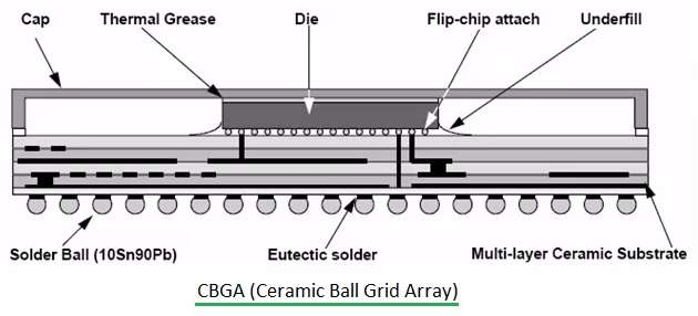
- CBGA: Ceramic Ball Grid Array
- CCGA: Ceramic Column Grid Array
- TBGA: Tape Ball Grid Array
- CSP: Chip-Scale Package
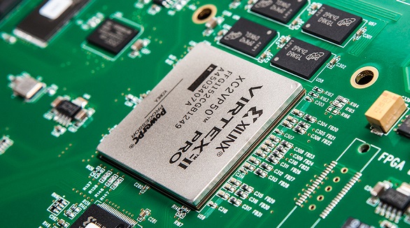
Each of these has its advantages and disadvantages, which we shall discuss.
Properties of BGA Components
Key properties that exist for ball grid array components include:
- High I/O Density: A more significant lead pitch can accommodate more I/O counts within the same area.
- Improved Reliability: A lower defect rate in solder joints; higher overall reliability in packaging.
- Easy to Align: Unlike QFP chips that rely on visual alignment, with their larger pin pitch, BGA components are easier to align and solder.
- Simpler Solder Paste Printing: Stencil-aided solder paste printing becomes easier with BGA components.
- Better Flatness: BGA pins lie flatter as compared to the QFP package, and the melting of solder balls corrects flatness errors automatically.
- Higher Self-Alignment: During soldering, the tension between the solder joints enhances self-alignment, which can tolerate mounting precision errors of as high as 50%.
- Excellent Electrical Performance: BGA components have good frequency characteristics.
- Best Thermal Dissipation: BGA components usually offer better thermal management.
However, there are several disadvantages to BGA components. One of the main issues is that it can be difficult to inspect the integrity of the solder junctions. AXI and AOI are necessary to monitor the collapse of the solder balls, which raises inspection costs and complications.

Storage and Application Environment of BGA Components
BGA components are susceptible to humidity and temperature changes. In turn, they should be stored in a dry environment with consistent temperature conditions. Ideally, the storage conditions should be 20°C-25°C, RH below 10%, and it is optimum to store these components in nitrogen gas.
Once opened, BGA component packages should be exposed to air for as little time as feasible. Use within 8 hours at ≤30°C/60%RH. If preserved in nitrogen, they can be used for an extended period of time.
If BGA components are not used directly after the packages are opened, baking is necessary to recover solderability. The baking temperature will generally be set at 125°C while the baking time will depend on the thickness of the package:
| Package Thickness t/mm | Baking Time h |
|---|---|
| t ≤ 1.4 | 14 |
| 1.4 < t ≤ 4.0 | 24 |
Too high a baking temperature will affect the joints' metallographic structure for the solder balls, cause floating, and decrease assembly quality. Alternatively, if it is too low, it cannot ensure dehumidification. The BGA components should be cooled for 30 minutes after baking before assembly.
BGA Component Soldering Technologies
The process of BGA component assembly is compatible with the SMT. The main phases of the soldering process are solder paste printing, component alignment, and reflow soldering. The outline of the PBGA soldering process is given below:
Printing of Solder-paste:
The quality of the solder paste may either ensure or destroy the soldering procedure. The solder paste should have good printability, solderability, and little contamination. The particle diameter corresponds to the pitch of the leads of the components. Fine-pitch BGA components require solder paste with particles smaller than 45μm.
Stencils for solder paste printing are made from stainless steel, usually thickness 0.12mm to 0.15mm. Lasers are used to cut the stencil openings, which are somewhat smaller than the pads.
Component Mounting:
Each BGA solder ball is aligned with PCB pads. Specialized equipment like BGA rework stations or chip mounters is used. Modern chip mounters have an accuracy of up to 0.001 mm using mirror recognition for accurate placement.
The height of the BGA components may be reduced to 25.41μm to 50.8μm for better solderability, and a delay shutdown vacuum system may be used for better contact between solder balls and solder paste.
Reflow Soldering:
Reflow soldering is also an equally important process. The optimum curve for reflow soldering should contain the following four phases: preheating, soaking, reflow, and cooling. The temperature and duration of each phase need to be strictly controlled if quality soldering is desired.
BGA Rework:
BGA rework stations can work on individual BGA chips without affecting the surrounding components. Hot air reflow nozzles of various diameters are widely used to solder the BGA chip on-site.
BGA Component Soldering Quality Inspection
A visual inspection is insufficient since the solder balls in a BGA component cannot be seen. X-ray inspection is commonly used to assess the quality of soldering. This is available in both 2D and 5D versions.
- 2D X-ray Inspection: It may discover defects like cracks, missing, bridging, misalignment, and insufficient solder at a reduced cost. This approach may fail to distinguish images that overlap each other.
- 5D X-ray Inspection: It provides finer inspection compared with the 2D limitation and at a higher cost.
PCBX will do 100% Inspection of Your BGA Components
Each BGA component is meticulously tested at PCBX prior to SMT assembly to ensure optimal performance in your final product. AOI or AXI inspection will ensure the quality of your BGA components. Please contact us if you would like more information about our inspection methods and supply chain management.
Hot Tags:
Contact us

If you can't find what you're looking for, please contact us.
Article

The article compares Ball Grid Array (BGA) and Land Grid Array (LGA) packaging technologies for mounting microprocessors on PCBs. It details their pros and cons, applications, and factors to consider for optimal design choices.
Ensuring BGA soldering quality involves defect prevention, pre-soldering measures, and precise control during SMT assembly and reflow soldering.
In the late 1980s, when electronics began to shrink, BGA packaging was developed to integrate more connections within a given area. Today, BGA is widely used with high-connection chips—processors being a good example. BGA uses solder balls at the bottom of the chip to connect it to the circuit board. It provides high density along with good heat dissipation and fast signal transmission, one of the main reasons it is ideal for modern electronics. However, it requires precise techniques of soldering in BGA manufacturing.