BGA Packaging Technology and Traditional SMT/SMD
Compared to THT, SMT offers better miniaturization and weight reduction in any electronic application. With the use of BGA packages, high-assembly density, reliability, and improved performance are achieved; on the other hand, this requires a rework and inspection that is not really common. PCBX specializes in the area of advanced SMT and BGA assembly to help drive modern requirements of compact electronic devices.
The surface mount technology is generally viewed as directly opposite to its traditional through-hole technology because, in relative comparison to THT assembly, the space is reduced by 60% to 70% and the weight by 70% to 80% since the electronic components are soldered directly on both sides of the PCB without drilling any holes. These, together, make SMT have a critical impact on miniaturization, lightness, and thinness in electronic products. In particular, for applications with fine-pitch SMT where the pitch is less than 0.65 mm, appliances such as cell phones, PCs, and video cameras show the trend.
SMDs come in various packages: SOP (Small Outline Package), LCC (Leadless Chip Carrier), PLCC (Plastic Leadless Chip Carrier), SOJ (Small Outline J-Lead) package, SOIC (Small Outline Integrated Circuit), QFP (Quad Flat Package), etc., of which QFP is the most commonly used. In a PLCC (Plastic Leaded Chip Carrier), there are either no leads from the device at all or very small leads coming from the package.
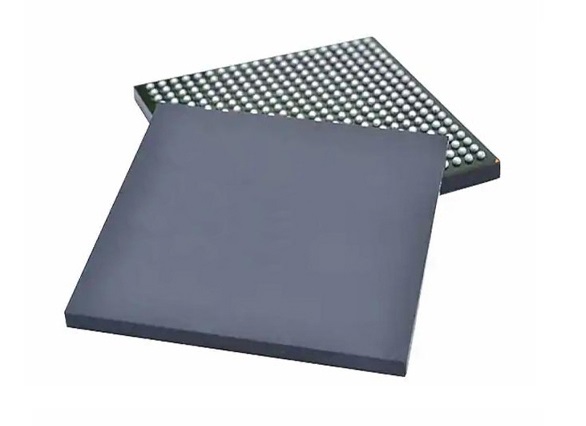
With constant aggressive innovations in IC, more functions with more I/O pins are demanded. Electronic products also have to be as dense as they can be. Conventional SMT packaging technologies, such as QFP, make it difficult for traditional technologies to meet these demands explicitly because of their inherent characteristics as the linearly distributed leads of QFP and the limit of pitch reduction of leads.
BGA packaging technology can provide a better solution. When there are a lot of I/O pins, it's difficult to maintain expanded functionality while also lowering product volume, eventually providing a symmetric solution. The BGA packages give way to the most technical breakthroughs in application and manufacturing.
• Comparing BGA Packaging Technology to Traditional SMT/SMD Packaging
Comparison of BGA packaging technology is also always provided with some views on traditional SMT/SMD packaging. Among them, the most important is lead structure.
| Items | Gull wing | J lead | I lead | BGA |
|---|---|---|---|---|
| Capability to adapt multi-lead package | Good | Ordinary | Ordinary | Excellent |
| Package thickness | Good | Ordinary | Ordinary | Excellent |
| Lead rigidity | Ordinary | Good | Ordinary | Excellent |
| Capability to adapt multi-soldering | Excellent | Ordinary | Ordinary | Ordinary |
| Self-alignment capability in reflow soldering | Good | Ordinary | Ordinary | Excellent |
| Capability to be inspected after soldering | Ordinary | Good | Ordinary | Ordinary |
| Cleaning difficulty | Ordinary | Good | Excellent | Ordinary |
| Effective area utilization | Ordinary | Good | Ordinary | Excellent |
• Comparison of Package Size
Three types of packages are used as comparison examples with their parameters displayed in Table 2 below.
| Package | Lead Count | Pitch(mm) | Package Size(mm) |
|---|---|---|---|
| BGA | 625 | 1.27 | 32*32 |
| TAB | 608 | 0.25 | 44*49 |
| PQFP | 304 | 0.5 | 46*46 |
Based on the parameter comparison in the above table, it’s obvious that BGA features the largest number of leads and the smallest package size.
• Assembly Density Comparison between All Types of Package Structures
Assembly density comparison between all types of package structures is summarized in Table 3 below.
| Package | Pitch (mm) | Size (mm) | I/O Pin Count |
|---|---|---|---|
| BGA | 1.27 | 32.5*32.5 | 625 |
| FPD | 0.5 | 32.5*32.5 | 240 |
| UFPD | 0.4 | 32.5*32.5 | 296 |
| UFPD | 0.3 | 32.5*32.5 | 408 |
| TCP | 0.25 | 32.5*32.5 | 480 |
| TCP | 0.2 | 32.5*32.5 | 600 |
• Assembly Procedure
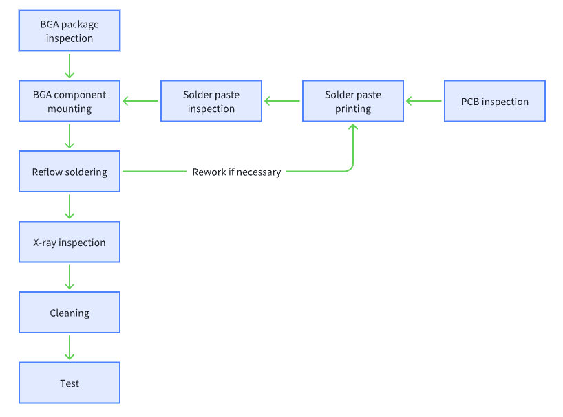
BGA (Ball Grid Array) package technology is an advanced version of the traditional SMT (Surface Mount Technology) packages, which explains the intrinsic advantages of SMT. Both the fine pitch components and BGA package components are assembled using a similar assembly procedure, which is indicated in the figure adjacent below.
• Assembly Defect Rate
BGA packages often have a lower defect rate and are more manufacturable than QFP peripherals.
• Final Inspection
Inspecting fine-pitch QFPs needs additional resources because reliability tests are necessary. Typically, an automated system is required for testing QFP short circuits or open circuits, which increases the cost of manufacturing them. The converse is true for BGA packages, which have a high manufacturing efficiency and a low defect rate. As a result, BGA inspections focus primarily on alignment and placement.
• Rework
Reballing BGA packages is generally more expensive than reworking QFP components for two reasons:
a. Because of the design, rewiring a single short or open circuit in a BGA is nearly impossible; hence, defect-free assembly is uncommon.
b. QFP rework is easier than BGA package rework. Frequently, reworking a BGA package necessitates the use of specialized equipment, which increases the cost.
c. BGA variations do not ensure post-rework functionality; however, some QFP components can be reused if thoroughly dismantled.
The basic comparison between BGA rework and typical SMT rework methods reveals that BGA rework requires full preheating. While the temperatures used for preheating BGA components are likewise used by other SMDs, they have a different temperature ramp rate or transit time between respective heating temperature points. Besides, the heating process for BGA components should be a gradual one if the preheating curve is smooth.
Second, all solder balls in the BGA must be heated simultaneously. Solder paste is precisely applied, and the solder junctions cannot be modified. BGA components have a large pitch, which makes depositing easier.
• Soldering Positions to Be Kept Reserved
The major difference between BGA and QFP in terms of reserved soldering position comes from their respective hidden array and lead configurations. Each enjoys a variety of benefits related to enhancing PCB design with superior trace density, tracing activity, and general performance.
Good heat dissipation properties of the BGA packages make them exhibit the best conditions even though the confinement in the PCB design rules demands narrow spacing between thermal parts.
• Solder Joint Reliability
The following are some of the factors that have a significant impact on board and assembly rates of solder joints: board solderability, component soldering performance, component coplanarity, and solder paste volume. The ultimate product's quality would be the result of these aspects being combined.
QFP is one of the traditional microelectronic packaging technologies. Technically speaking, it is already going to give way to one modern packaging technology as far as new expectations: the feature sets and I/O pin counts.
PCBX Specializes in BGA and other types of SMD Assembly
With over two decades of industry expertise, PCBX has successfully assembled electrical components of various packaging types, including BGA, QFN, QFP, CSP, WLCSP, and so on. We can construct SMDs in the PCBX workshop starting with 01005, with a minimum pitch of 0.4mm for BGA and 0.35mm for WLCSP. It is consistent with the current trend of miniaturizing electronics.
With our Advanced PCB Assembly services, we can offer many more, so do not hesitate to get in touch. Quotations are free and always welcome.
Hot Tags:
Contact us

If you can't find what you're looking for, please contact us.
Article
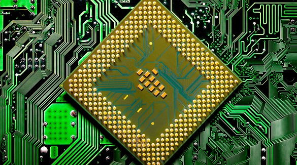
BGA assembly, challenging due to hidden joints and warpage, requires advanced techniques, skilled training, and strategic planning for reliable PCB production and minimized defects.
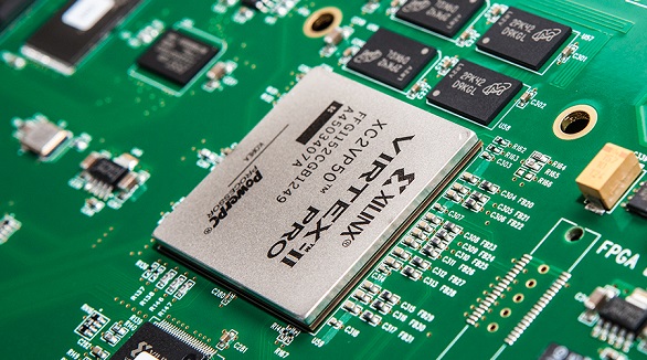
Ball Grid Array (BGA) components, such as PBGA, CBGA, CCGA, TBGA, and CSP, provide high I/O density, improved reliability, and high-quality electrical and thermal performance. Quality assembly and functionality are assured since advanced soldering and inspection methods are required, like AXI and AOI. Proper storage and handling shall guarantee the performance of the devices.
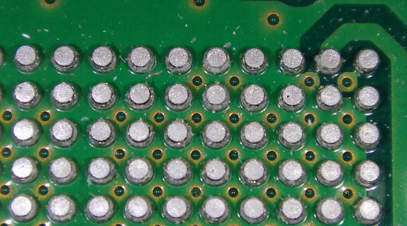
In the late 1980s, when electronics began to shrink, BGA packaging was developed to integrate more connections within a given area. Today, BGA is widely used with high-connection chips—processors being a good example. BGA uses solder balls at the bottom of the chip to connect it to the circuit board. It provides high density along with good heat dissipation and fast signal transmission, one of the main reasons it is ideal for modern electronics. However, it requires precise techniques of soldering in BGA manufacturing.
