- Products & Capabilities

- About
- Resources
BGA


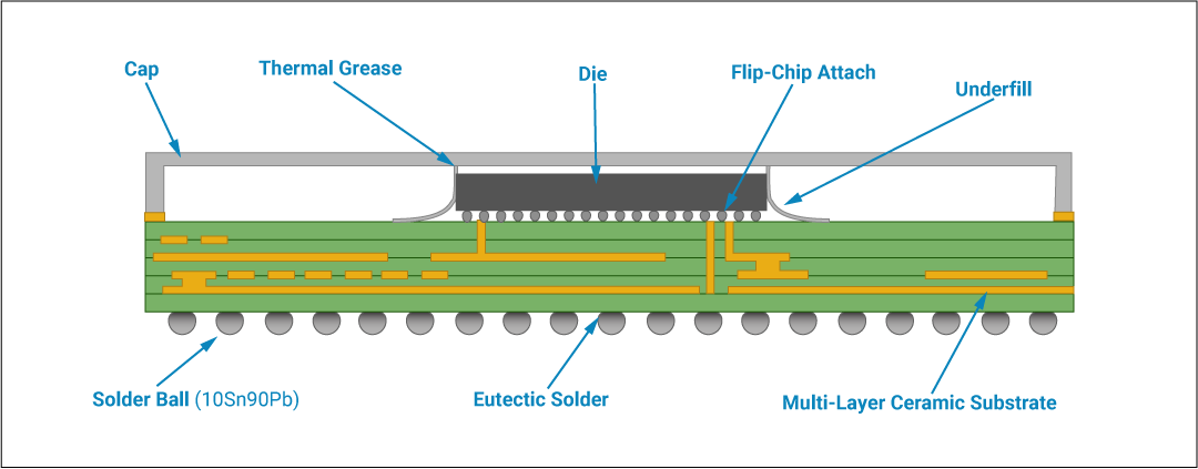
In the late 1980s, when electronics began to shrink, BGA packaging was developed to integrate more connections within a given area. Today, BGA is widely used with high-connection chips—processors being a good example. BGA uses solder balls at the bottom of the chip to connect it to the circuit board. It provides high density along with good heat dissipation and fast signal transmission, one of the main reasons it is ideal for modern electronics. However, it requires precise techniques of soldering in BGA manufacturing.
As electronics becomes smaller, so did the space for components. BGA packaging emerged in the late 1980s, offering a solution. Compared to older options, BGA packs more connections in a smaller space, keeps costs similar, and avoids manufacturing hassles. Today, BGA is the go-to choice for high-connection chips like processors and storage.
What is BGA?
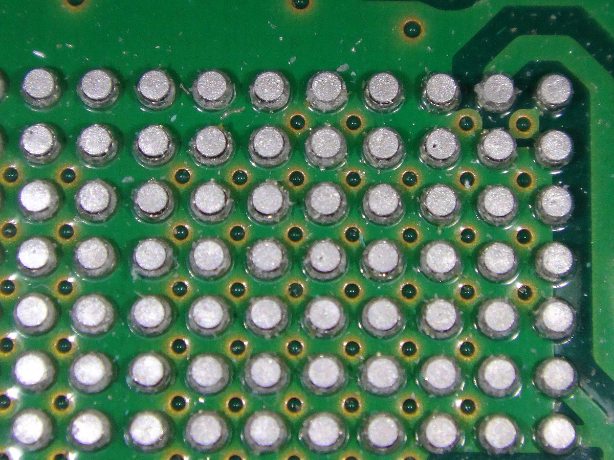
BGA is "Ball Grid Array," which refers to a PCB with a ball grid array structure, integrated circuit packaging method that uses an organic carrier. PCBs with BGA typically have smaller holes, with the finished holes under the BGA usually designed to have a diameter of 8-12 mil. The vias beneath the BGA must be plugged, and the pads should remain ink-free and undrilled.
Design Guidelines for BGA Pads
- The pad diameter is usually 20%-25% smaller than the solder ball diameter, which maximizes the routing space between the pads.
- The pads on the BGA substrate and the PCB are the same diameter.
- BGA pad design must ensure a stencil opening for 0.08mm³ of solder paste to ensure reliable solder joints.
Processes of BGA Packaging Technology
The main process flow of BGA packaging includes solder ball production, substrate manufacturing, die attachment, encapsulation and curing, and packaging separation.
- Solder Ball Production: High-purity tin-lead alloy or lead-free materials produce solder balls, forming a regular ball grid array.
- Substrate Manufacturing: Multi-layer printed circuit boards are used as substrates to achieve high-density, high-performance electrical interconnections.
- Die Attach: The die is connected to the substrate and attached using lead-free or lead-based solder.
- Encapsulation and Curing: The die is encapsulated with epoxy resin to protect it from environmental impacts.
- Packaging Separation: The encapsulated chips are cut into individual BGA packages.
Types of BGA Packages
BGAs, those tiny packages powering your devices, come in different flavors! Here's a quick guide:
- PBGA: Affordable, plastic-coated with etched copper traces. Ball pitch: 1.0 mm, 1.27 mm. 2-4 layered boards of organic matter.
- FlipChip BGA: Flips the chip for better performance, using a hard, multilayered base.
- CBGA: The tough guy - ceramic substrate for heat resistance in demanding applications.
- CSPBGA (Cavity Down PBGA): PBGA with a tiny cavity for heat dissipation in compact devices.
- TBGA (Tape BGA): Flexible, strip-shaped for space savings and movement.
- H-PBGA (High-thermal BGA): Built for heat dissipation with special materials, ideal for high-power electronics.
Advantages and Disadvantages of BGA
- Advantages
- High Density: BGA packages offer larger pitch spacing, enabling a higher number of I/O pins to meet the demands of high-performance integrated circuits.
- Superior Signal Transmission Performance: Due to the shorter connection paths of solder balls, BGA packages exhibit lower parasitic inductance and capacitance, facilitating high-speed signal transmission.
- Excellent Thermal Performance: The solder balls in BGA packages effectively conduct heat, helping to reduce the working temperature of the chip.
- Disadvantages
- Demanding Manufacturing Processes: BGA packages require stringent soldering processes and equipment, adding to production costs.
BGA packaging is a surface mount technology characterized by forming a regular array of spherical pins on the bottom of the package. This packaging method offers advantages such as larger pin pitch, good thermal performance, and excellent signal transmission capabilities, making it widely used in high-speed, high-performance integrated circuits. Its versatility and performance make it a technology of choice for a wide range of applications.
Hot Tags:
Contact us

If you can't find what you're looking for, please contact us.
 2024/07/24