- Products & Capabilities

- Simulation Design & EDA

- About
- Resources
Blind Via and Buried Via


A printed circuit board includes a number of copper foil circuits, which are interlinked by vias. Via (through-hole, blind, buried, stacked, microvias) provides critical interlayer connections in high-density interconnection boards. Blind and buried vias increase the density of boards without adding size; hence, they are imperative for modern trends of miniaturization and high-speed signal transmission. These vias are plated with conductive materials, usually copper, so the electron flow can happen without much effort. Although advanced via types, like stacked vias, cost more, they save up much space and significantly improve routing capacity.
A printed circuit board is made of several copper foil circuits laid on top of one another and connected by vias, which play an important role in providing solutions to interlayer connection challenges. If one will, one can also consider this as an underground system of waterways. One can even push the analogy further to those who have spent countless hours playing the video game Super Mario Bros. The idea is the same in that there are pipes, but the principle is different in that whereas the pipes are meant to bring water, the vias are meant to allow electricity to pass through. It does not conduct electricity intrinsically when the machine or laser drilled holes because its surfaces are made of non-conductive resin. To fix this problem, a layer of conductive material is plated onto the surface of the drilled hole; normally copper is used to allow the electrons to flow across different copper foil layers.
What is a Via?
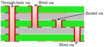
Vias are the copper-plated holes in the PCB that connect the different layers of the board. The most traditional type of vias is the through-hole via, although this type has several disadvantages if used on SMT. Therefore, blind vias or buried vias are often used instead. Blind or buried vias may be processed in different ways, and some are plugged copper mask vias, plated solder mask vias, plated vias, or staggered vias.
• What is Blind Via?
A blind via is simple or complex via that connects the external layer of the PCB to one or more inner layers, which facilitates interlinking between the surface and the inner layers of the board.
• What is Buried Via?
A buried via connects only the inner layers of the board and invisible from the outside. Such a via will be "buried" inside the board's inner layers.
Blind and buried vias are particularly useful in HDI boards since they increase board density without increasing the size of the board or adding more layers.
• What is Stacked Via and Microvia?
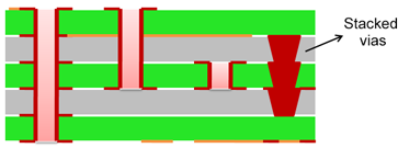
A stacked via takes it to the limit in size and density considerations in the manufacture of printed circuit boards — specifications that have become very critical given present miniaturization trends and high-speed signal transmission demands.
Unless the aspect ratio of the blind via is greater than 1:1 or the drilling requirements for the needs span multiple layers, the stacked via can provide a reliable internal connection.
Stacked vias are created utilizing laminated blind or buried vias. In other words, these are multiple vias contained in a circuit board constructed around the same center. Conversely, staggered vias are essentially laminated vias that lack a common center. Advantages of stacked vias include space savings, increased density, inner connection flexibility, better routing capacity, and reduced parasitic capacitance. The negative side includes the higher cost when compared with standard through-hole or blind/buried vias.
A microvia is simply a very small via. Due to their small diameter, microvias are very useful to PCB designers since they allow more routing space and less parasitic capacitance necessary for high-speed circuits. They require, however, more drilling time and are more demanding in terms of accuracy.
Contact PCBX for PCBs with Diverse Vias
High experience in blind and buried vias PCB fabrication: PCBX is completely prepared to provide exact blind via or buried via PCB that you need. The design parameters for PCBX's blind and buried vias are listed below.
Via Type Via Diameter
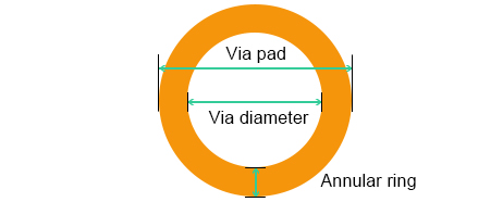
| Via Type | Via Diameter (max.) | Via Diameter (min.) | Via Pad | Annular Ring | Aspect Ratio |
|---|---|---|---|---|---|
| Blind via (mechanical) | 0.4mm | 150μm | 450μm | 127μm | 1:01 |
| Blind via (laser) | 0.1mm | 100μm | 254μm | 150μm | 1:01 |
| Buried via (mechanical) | 0.4mm | 100μm | 300μm | 150μm | 1:10 |
| Buried via (laser) | 0.4mm | 100μm | 225μm | 150μm | 1:12 |
Get in touch with us today to know more about via types and how we will optimize your PCB for the best performance. Click the button below for a free quote.
Hot Tags:

Contact us

If you can't find what you're looking for, please contact us.
Article
Vias—blind, buried, and through-hole—are essential in multi-layer PCBs, enabling signal and power transfer between layers. Covering techniques like tenting and plugging with solder masks enhance PCB reliability and performance, crucial for compact designs.
 2024/09/11
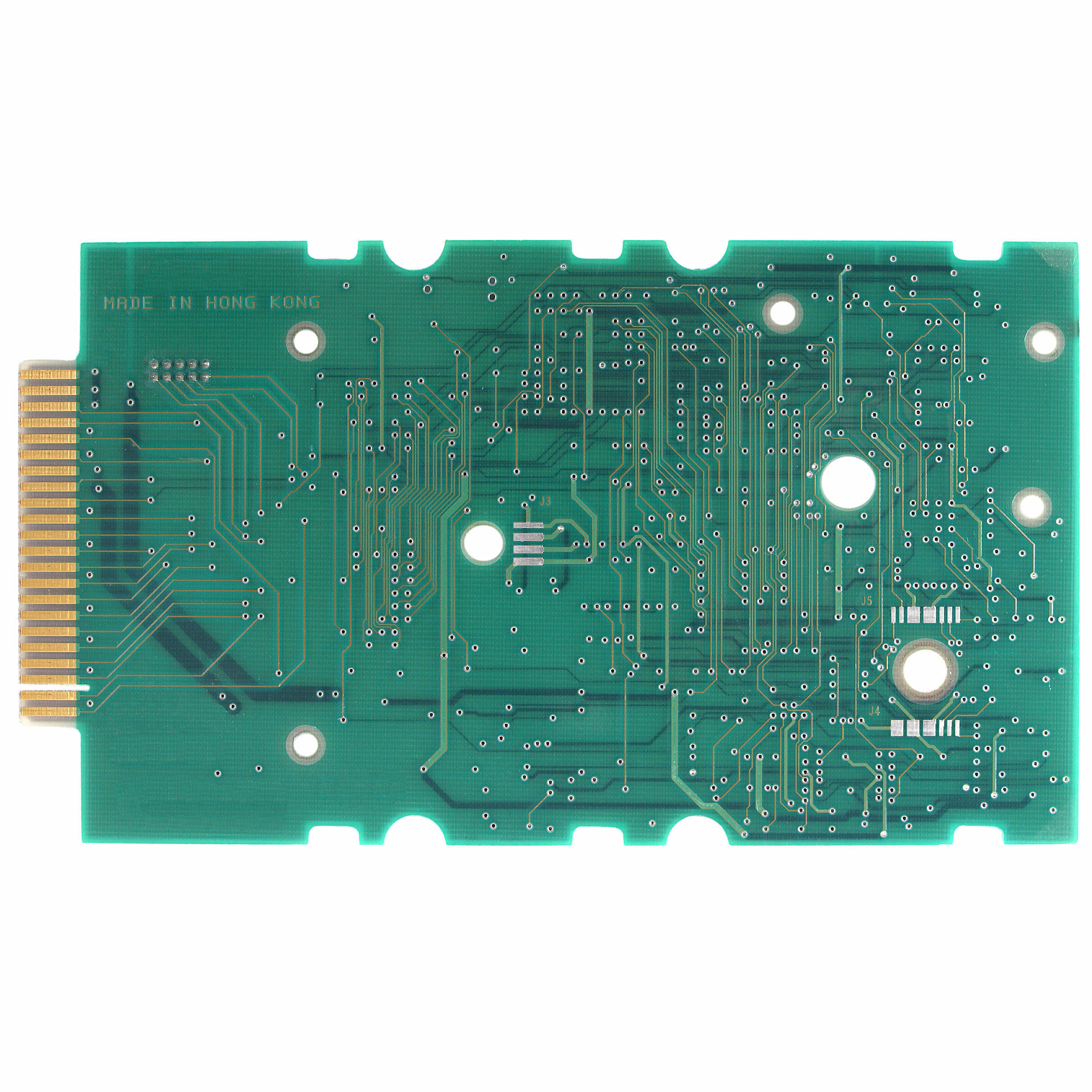
Backdrill in PCBs removes stubs in vias to improve signal integrity and impedance control, crucial for high-frequency, multilayer boards. It’s vital in communication, servers, medical, and aerospace applications.
2024/08/01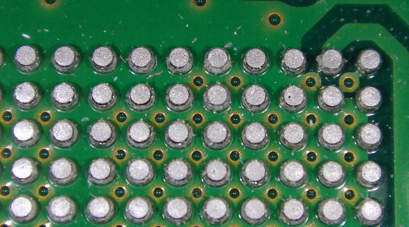
In the late 1980s, when electronics began to shrink, BGA packaging was developed to integrate more connections within a given area. Today, BGA is widely used with high-connection chips—processors being a good example. BGA uses solder balls at the bottom of the chip to connect it to the circuit board. It provides high density along with good heat dissipation and fast signal transmission, one of the main reasons it is ideal for modern electronics. However, it requires precise techniques of soldering in BGA manufacturing.
2024/07/24