Brief Introduction to High-Speed PCB Design
High-speed PCBs (>1GHz) are crucial for advanced electronics like 5G and data processors. Key practices include ensuring signal integrity, controlling EMI, and maintaining power integrity for reliable performance.
High-speed PCB design has become an essential part in today's advanced electronics, where the best performance with signal integrity is expected. The general understanding of high-speed printed circuit boards is that they operate at frequencies higher than 1GHz for signal transmission and find their applications in data processors, radar systems, automobiles, and the latest 5G technology, among others. This guide walks through the key principles and best practices in the design and manufacturing of high-speed PCBs, ensuring their reliable performance in the most advanced electronic systems.
What is a High-Speed PCB?
A high-speed PCB is designed to bear signal transmission frequencies over 1GHz. Unlike other usual PCBs, which do not require much regarding technical specifications, advanced materials, and design techniques, a high-speed PCB requires them all. These attributes make PCBs very important in applications that need fast and stable data transmission.
Some of the key characteristics that make these high-speed PCBs different from others include:
DK and DF: Dielectric Constant and Dissipation Factor, respectively, are significant in maintaining transmission speed and signal stability.
Water Absorption: Smaller values of water absorption reduce DK and DF, which is an essential condition to achieve quality signal transmission.
Impedance Control: Impedance control allows high quality signal transmission.
High-Speed PCB Design Guide
Designing a high-speed PCB requires great planning with accurate execution. Following are the key considerations and guide to help in designing:
Layers and Stack-Up
The number of layers and size of the PCB, the placement of BGA components, is very crucial in the design of high-speed PCBs. All these parameters verified as early as possible enable better stack-up structure and impedance control, hence making it very important for high-performance PCBs.
Layer Confirmation: Confirm the number and size to facilitate proper stack-up and impedance control.
Layer Reservation: A little margin in layer count while designing gives space for functional modifications in the future without redesign.
Signal Integrity
Perhaps the most critical issue in high-speed PCB design is signal integrity, which actually determines if the data is going to be transmitted accurately and the overall performance is going to be reliable.
Controlled Impedance: Design consistent impedance traces by adjusting trace widths, spacing, and stack-up.
Termination Techniques: Use appropriate termination resistors to minimize signal reflections.
Short Signal Paths: The high-speed signals must have the shortest paths to lessen their degradation.
Electromagnetic Interference (EMI)
High-speed circuits tend to emit EMI easily and interfere not only with all other electronic devices, but also with the PCB itself.
Ground Planes: Use continuous ground planes for low impedance return paths.
Shielding Techniques: Employ copper pours and shielded layers for effective EMI containment.
Filter Components: Filters can be used to smoothen high frequency noise.
Power Integrity
Stable feeding is required in order to avoid noise and signal integrity problems for operating high-speed circuits reliably.
Power and Ground Planes: A separate plane reduces voltage drops and noise coupling.
Decoupling Capacitors: Locate them near power pins to keep voltages stable and to filter out noise.
PDN Design: The Power Distribution Network should be designed such that it can supply transient current requirements.
Crosstalk
Crosstalk A signal in one trace can induce voltages in adjacent traces and may cause data errors or loss of performance.
Trace Spacing: Space high-speed traces farther apart to reduce coupling.
Orthogonal Routing: Route signal layers perpendicularly to reduce parallel coupling.
Guard Traces: Employ grounded guard traces around critical signals to isolate them.
Differential Pair Routing
Differential signaling involves the use of trace pairs carrying signals in opposite phases, improving noise immunity and reducing EMI.
Matched Lengths: Match the lengths of differential pairs to avoid signal skew.
Consistent Spacing: Allow spacing to be consistent to maintain differential impedance.
Symmetry: Route differential pairs symmetrically to avoid imbalance.
Component Layout and Placement
In a high-speed PCB design, proper component layout is significant in ensuring signal integrity and minimum EMI.
Component Prioritization: Prioritize the layout to accommodate high-speed components.
Signal Path Optimization: Make paths for high-speed signals as short as possible.
Minimise Vias: In case of need, use microvias for minimizing impedance variation and reflection.
Fan-out Design
Fan-out design means the process of connecting each and every pin to a via. Fan-out design empowers the connection to inner PCBs and enhances testability.
Via Sizing: Use maximum via size for better performance of the circuit and test accuracy.
Test Fixture Development: Design and fabricate a test fixture concurrently with the development of the PCB, while at the same time being able to use it proficiently when the board is available.
Wiring Layout
Final wiring layout will help in keeping the length of the signal path as short as possible to make it functional.
Shorten Long Lines: Shorten extremely long signal traces.
Rewire: Make changes in wiring if necessary to achieve best routing of signal and signal integrity.
Conclusion
High-speed PCB design is one of the complex but essential activities in obtaining optimal performance and reliability in new electronic devices. Understanding and addressing crucial parameters like signal integrity, EMI, power integrity, and crosstalk and adaptability to best design practices have been helping in the manufacture of quality high-speed PCBs. Advanced design principles and taking advantage of state-of-the-art fabrication technologies will lead to innovations in electronic applications.
Hot Tags:
Contact us

If you can't find what you're looking for, please contact us.
Article
Designing a PCB involves ten detailed steps: schematic capture, creating a blank PCB layout, syncing designs, defining stackup, setting design rules, placing components, adding drill holes, routing traces, labeling, and generating output files. These steps ensure an organized, error-free process from concept to manufacturing.
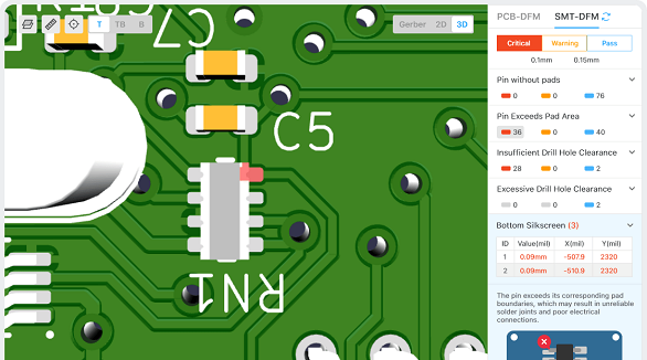
The article is developed concerning the breakthrough of integrated circuits and the need for custom PCBs in some electronic products. It enumerates ten golden rules in conducting PCB layout design and manufacturing: grid selection, routing, power layers, component placement, panel duplication, component value combination, frequent DRC, flexible silkscreen use, decoupling capacitors, and pre-production parameter checks. These rules provide for the optimum design and manufacturing of a PCB.
The article explains the current situation of Printed Circuit Boards and future development based on efficient production helped by advanced software and manufacturing processes. Future technological developments are in store for 3D Printed Electronics, flexible PCBs, eco-friendly biodegradable PCBs, and board cameras. It elaborates on other powerful automation tools that are going to make the entire PCB design process efficient in the near future. All of them will further improve and develop with the technological advances in PCBs, keeping up with the ever-increasing industry and consumer demands.