- Products & Capabilities

- About
- Resources
Common Challenges and Solutions in Reflow Soldering


Reflow soldering is vital for PCB assembly but faces challenges like solder bridging, tombstoning, and voiding. Effective solutions include optimized stencil design, thermal profiling, and precise component placement.
Reflow soldering is a very critical process in surface mount technology PCB assembly. In fact, it provides many advantages: accuracy in component placing, solder joint quality, and productivity. Nevertheless, every complex process has its problems and complications. This article tries to outline some generally faced problems with reflow soldering and lists certain effective ways to defeat these issues as a guarantee for top-quality PCB assemblies with consistent and reliable solder joints.
Reflow Soldering Common Challenges
Solder Bridging
Challenge
The problem of solder bridging occurs when excess solder bridges two adjacent pads or components together, unwanted shorts that may cause malfunctioning on the board.
Solution
Stencil Design: Proper stencil design with appropriate aperture sizes and thickness can control the amount of solder paste deposited, reducing the possibility of bridging.
Solder Paste Volume: Properly controlling the volume of solder paste applied avoids over-solder, which may cause bridging.
Reflow Profile: Optimizing the reflow profile will afford a better flow control of the solder paste to wet the intended pads only and without bridges.
Tombstoning
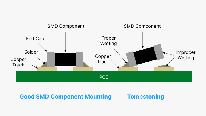
Challenge
Tombstoning-or the Manhattan effect-is a condition wherein one end of a surface-mount component lifts off the pad during reflow. This usually occurs due to uneven heating or differences in pad size.
Solution
Thermal Profiling: Necessary care shall be taken in considering thermal profiling. Tightening up temperature ramp-up, soak, and cooling rates can provide uniform heat across the PCB and reduce thermal stresses.
Pad Design: Proper design and size of the pad should match the component. This reduces any wetting force imbalance.
Component Placement: Employment of a pick-and-place accurate machine with a vision system for precise placement can reduce the possibility of tombstoning.
Voiding
Challenge
Voiding implies gas pockets or voids within the solder joint that can compromise mechanical strength and thermal conductivity.
Solution
Solder Paste and Stencil Design: Control of paste deposition by optimizing stencil design and selecting solder pastes that offer low voiding characteristics is paramount.
Reflow Profile: The reflow profile may be refined to balance preheat and soak stages, allowing adequate outgassing to take place, which could minimize voids.
Vacuum Reflow Ovens: Application of vacuum pressure to the molten solder by the use of vacuum reflow ovens would help to remove voids.
Component Misalignment
Challenge
Some forces, such as vibration or air flow during reflow, may cause misalignment of the components by improper placement, thus leading to assembly failures.
Solution
Placement Accuracy: Place the components accurately and reliably by using calibrated pick-and-place machines.
Reflow Parameters: Optimize parameters of the reflow oven to reduce disturbing forces that may displace components.
Paste Viscosity: Apply solder paste of the right viscosity that can keep the component in its place while reflow takes place.
Inadequate or Excessive Deposition of Solder Paste
Challenge
Poor deposition of the solder paste may result in weak and incomplete solder joints due to lack of paste, or bridging occurs with excessive paste.
Solution
Stencil Design and Quality: Stencils used must be of high quality to have proper aperture size and thickness for correct control over the volume of solder paste.
Printing Techniques: Printing parameters like squeegee pressure, speed, and angle are very critical and shall be optimized to uniformly apply the paste.
Inspection Systems: Implement automated solder paste inspection systems that can ensure solder paste volume accuracy and identify any anomalies.
Thermal Profile and Cycling Effects
Challenge
The high temperatures the product is subjected to during reflow may cause thermal stresses that can potentially damage temperature-sensitive components and lead to defects such as solder joint failure and voids due to thermal variations.
Solution
Thermal Management: Employ methods such as, but not limited to thermal vias, heat sinks, and thermal relief patterns to evenly distribute the temperature within the PCB.
Component Selection: Specify component parts with compatible coefficients of thermal expansion to limit resultant mechanical stresses.
Gradual Heating and Cooling: Optimize the reflow profile to achieve controlled and uniform rates of heating and cooling, tending in general to minimize thermal gradients and warping of the component surface.
Head-in-Pillow Defects
Challenge
Head-in-Pillow defects are those where the solder paste partially wets the component pad but does not wet the corresponding PCB pad, leading to poor joint integrity.
Solution
Stencil Aperture Design: Step stencils or optimization of aperture ratios will improve solder paste release.
Reflow Profile: Adjust the reflow profile for proper wetting and flux property activation.
Selection of Solder Paste: The solder pastes shall be selected based on formulation to give minimum voids and providing improved wetting characteristics.
Conclusion
RefLow soldering offers a range of benefits for the assembly of PCBs but is equally fraught with a number of key challenges to achieve good solder joints. Knowledge of such challenges combined with effective solutions thus enables optimization of the reflow soldering processes to manufacture reliable and robust PCB assemblies.
Proper stencil design and inspection, together with periodic maintenance and calibration of the reflow equipment, are performed to avoid solder bridging and component damage. That ability to continuously monitor and refine the reflow process enables a manufacturer to provide consistent, high-quality results-a driving factor behind the success and reliability of modern-day electronics.
By adopting these methods and best practices, you can easily override the challenges related to reflow soldering and result in quality PCB assemblies that bring along better performance and reliability.
Hot Tags:

Contact us

If you can't find what you're looking for, please contact us.
Article
Wave soldering is vital for assembling printed circuit boards (PCBs), aiming to bond electrical components. The process involves passing PCBs over a wave of molten solder to form connections. Common defects include pin/blow holes, solder shorts, poor hole fill, lifted components, excessive solder, solder balling, and solder flags. To address these issues, key factors include proper flux application, controlled preheat temperatures, optimal solder wave settings, and careful material handling. Understanding and managing these factors ensures high-quality, reliable PCB assemblies.
 2024/09/05
Solder masks protect PCBs from environmental damage and electrical shorts, enhancing reliability and aesthetics. The application is complex, requiring professional fabrication to ensure quality and compliance with regulations.
2024/08/20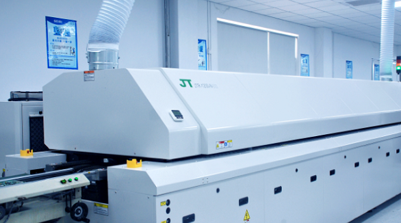
Soldering forms a very important part in the assembly of a PCB. Wave soldering is ideally applied in Through-Hole Technology, while reflow soldering in Surface Mount Technology. Wave soldering involves flux spraying, pre-heating, soldering, and cooling, while in the case of reflow soldering, pre-heating, thermal soak, soldering, and cooling steps are applied. Temperature and time control are the two most critical parameters in the above-mentioned techniques for ensuring soldering reliability.
2024/07/26