- Products & Capabilities

- Simulation Design & EDA

- About
- Resources
Comparison of AOI, ICT, and AXI


These SMT PCB assembly methods are involved, ensuring that several defects are detected. This includes the use of Automated Optical Inspection, In-Circuit Testing, and Automated X-ray Inspection. The combination of these methods is beneficial in facilitating an optimal inspection process.
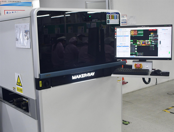
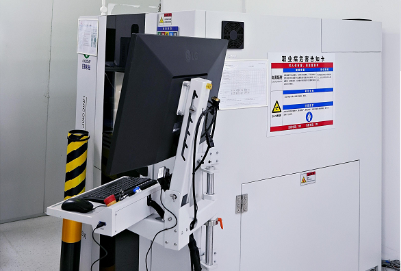
Automated Optical Inspection (AOI)
AOI has increasingly resembled a traditional inspection technique that is quickly expanding in SMT PCB assembly. Under the AOI technique, the spinning camera captures photos of the PCB, which are then compared to predetermined parameters recorded in a database. This technique is, therefore, a method of image processing with the capability of detecting defects present on PCBs that have undergone surface mounting. These flaws are then shown or highlighted for identification via a monitor or automatic markers, which otherwise assist rework staff in efficiently addressing them.
- Final Quality Inspection:
- Prior to the product exiting the production line, it involves a state check. This type of examination is crucial in situations where the product's quality is in doubt, and there are obvious manufacturing flaws, or the SMT PCB assembly calls for a high mix—that is, when speed and quantity are crucial factors. AOI equipment is often located at the end of the assembly line, where it provides extensive information for process management.
- Process Monitoring:
- AOI equipment observes the SMT assembly process, classifying defects with detailed defective characteristic information about the mounting displacement of components. This objective comes into existence in the sense that product reliability is an issue or when high-volume and low-mix assembly is done to provide continuous component supply. To provide real-time situation information and to make necessary adjustments, AOI equipment is used at quite a large number of positions on an assembly line so that effective process monitoring can be achieved.
- While AOI equipment can be sited at many positions along the manufacturing line, it should be located where it can detect and correct the maximum number of defects. Three key inspection locations are:
- After Solder Paste Printing:
- It detects defects such as insufficient or excessive solder paste, misalignment between the solder paste and pads, and solder bridging. Good placement ensures that the more probable defects at an early stage are noticed and minimized to minimize the chances of occurrence during later test stages like In-Circuit Testing.
- Before Reflow Soldering:
- This position picks up all those defects originating from solder-paste printing and component mounting and provides process tracking and alignment calibration for IC and fine-pitch component mounters.
- After Reflow Soldering:
- Placed at the final phase of surface mounting, AOI equipment can identify comprehensive assembly issues, providing a higher level of security since it detects defects from all the preceding stages.
In-Circuit Testing ICT
ICT equipment is a basic electrical test equipment that involves the use of a bed-of-nails to create contact with the soldered components in a PCB. It applies individually specific voltages and currents in testing for defects such as missing or misaligned components, deviations in parameters, solder joint bridging, opens, and shorts. Bed-of-nails ICT is fast and low-cost when testing simple PCBAs and high-volume production. On the other hand, it has huge limitations with high-density and complex circuits.
The flying probe test uses many probes to test circuit electrical performance and is particularly useful for SMT PCB assembly and fabrication tests. This methodology presents the advantages of flexibility and detailed examination of complex circuits.
Automated X-ray Inspection (AXI)
AXI is a fairly new examination technique. X-rays are absorbed by a detector as they pass through AXI equipment. These lead-rich solder junctions appear in the images as dark spots, highlighting the faults plainly and directly. Modern AXI technology has advanced from two-dimensional to three-dimensional examinations of single- and double-sided boards. It can inspect hidden solder junctions, such as BGAs (Ball Grid Arrays) and PTHs (Plated Through Holes), for quality assurance.
Now, solder joint defects can be inspected intricately with the advancement to 3D X-ray inspection, greatly improving the quality control of the assembly process.
Comparison of AOI, ICT, and AXI
ICT:
- Advantages: High capability of defect detection and test speed, suitable for mass production.
- Disadvantages: Little flexibility for low volume and diverse products; high-density circuits and complex test points are a challenge.
AOI:
- Advantages: Quick production of test programs and high flexibility. It collects production quality data and defect kinds for analysis and control.
- Disadvantages: No Detection of circuit error, small possibility to inspect hidden solder joints.
AXI:
- Advantages: Very high coverage of manufacturing defects (up to 97%), able to inspect hidden solder joints.
- Disadvantages: No testing of defects that relate to electrical performance is possible.
Inspection Methods—Optimized Utilization
Since the three methods have very distinct advantages and limitations, ICT, AOI, and AXI are not mutually exclusive but complementary. While ICT focuses on circuit defects, AOI and AXI target appearance defects. A combination of these various methods will enhance the inspection process as a whole.
Hot Tags:

Contact us

If you can't find what you're looking for, please contact us.
Article
As PCB lines and components shrink, traditional visual inspection fails; AOI using DRC and CAD methods is crucial for quality SMT assembly, offering intelligent, accurate inspections.
 2024/08/08
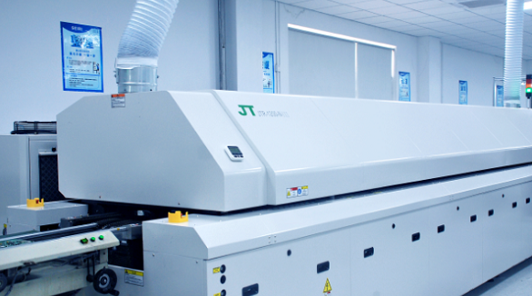
Soldering forms a very important part in the assembly of a PCB. Wave soldering is ideally applied in Through-Hole Technology, while reflow soldering in Surface Mount Technology. Wave soldering involves flux spraying, pre-heating, soldering, and cooling, while in the case of reflow soldering, pre-heating, thermal soak, soldering, and cooling steps are applied. Temperature and time control are the two most critical parameters in the above-mentioned techniques for ensuring soldering reliability.
2024/07/26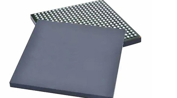
Compared to THT, SMT offers better miniaturization and weight reduction in any electronic application. With the use of BGA packages, high-assembly density, reliability, and improved performance are achieved; on the other hand, this requires a rework and inspection that is not really common. PCBX specializes in the area of advanced SMT and BGA assembly to help drive modern requirements of compact electronic devices.
2024/07/26