Comprehensive Guide to IC Packaging: Essential for Your PCB Designs
IC packaging is essential in electronics for protecting components, providing electrical connections, and managing heat. This tutorial explores its complexities, including its importance, various types like SMD, QFP, and BGA, and considerations for choosing the right package for specific applications. Proper IC packaging enhances PCB performance and reliability.
In the realm of electronics, one of the most important processes involves chip packaging. This is where all electronic components are used, such as chips, transistors, resistors, and capacitors, molded in forms and sizes for ease of use, hence mounted easily on a printed circuit board, offering considerable mechanical protection, providing electrical connections, and offering good thermal management. This tutorial takes an in-depth look into the complexities of IC packaging, covering its importance, common types, and aspects one considers when choosing the right package for one's application.
What is IC Packaging?
The packaging of ICs acts as the final stage in the process of semiconductor device fabrication. It encapsulates the fragile silicon die in which a functional circuit is fabricated within a protective case for protection from physical damage, corrosion, and environmental factors such as moisture and dust. The packaging process also allows for electrical interconnections between IC and the PCB and thermal management for efficient operation.
Importance of IC Packaging
Protection: It safeguards the integrated circuitry against mechanical damage and environmental influence.
Electrical Connection: It provides the pins or leads through which the IC is connected with other circuits.
Thermal Dissipation: It helps to dissipate the heat produced by IC functioning.
Form Factor: Assorted sizes and shapes render it suitable for different applications.
Common Types and Sizes of IC Packages
IC packages are categorized based on their application area and functional capabilities. Common categories include the following :
Surface Mount Device (SMD)
SMD packages are for Surface Mount Technology, where components are directly mounted onto the surface of a PCB without protruding pins.
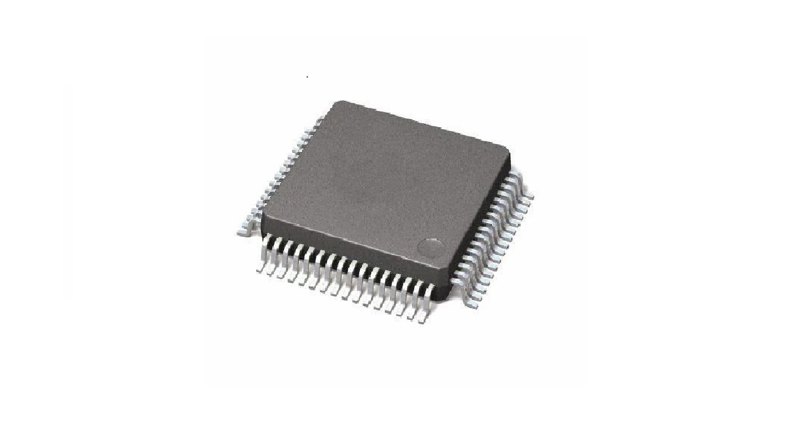
Quad Flat Package (QFP)
Description: The QFP has a larger PCB outline in both length and width with pins on all four sides.
Sizes: The common sizes include 7x7mm, 10x10mm, 14x14mm.
Pin Count: Ranges from dozens of hundreds.
Applications: It is used for ICs, integrated circuits, microcontrollers, and processors.
Ball Grid Array (BGA)
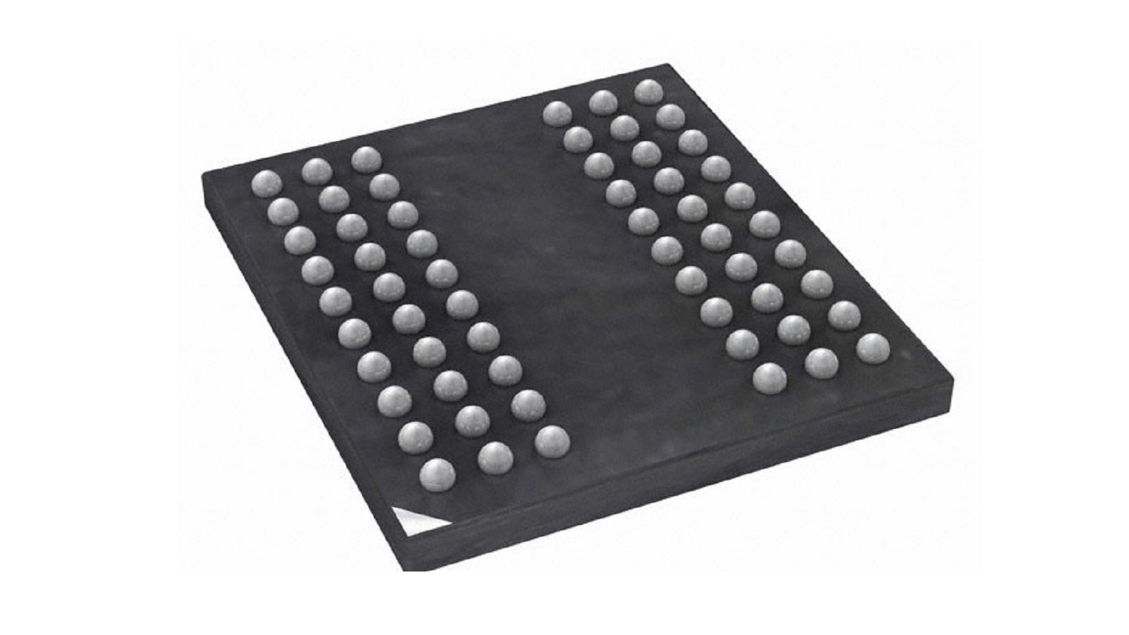
Description: A BGA package has a grid of solder balls underneath.
Pitch: 0.75mm to 1.0mm, and general usage pitches fall within this range.
Pin Count: Ranges from dozens of pins to hundreds of pins.
Features: It provides excellent heat dissipation and electrical performance.
Application: Apply to high performance and large-scale integrated circuits.
Small Outline Integrated Circuit (SOIC)
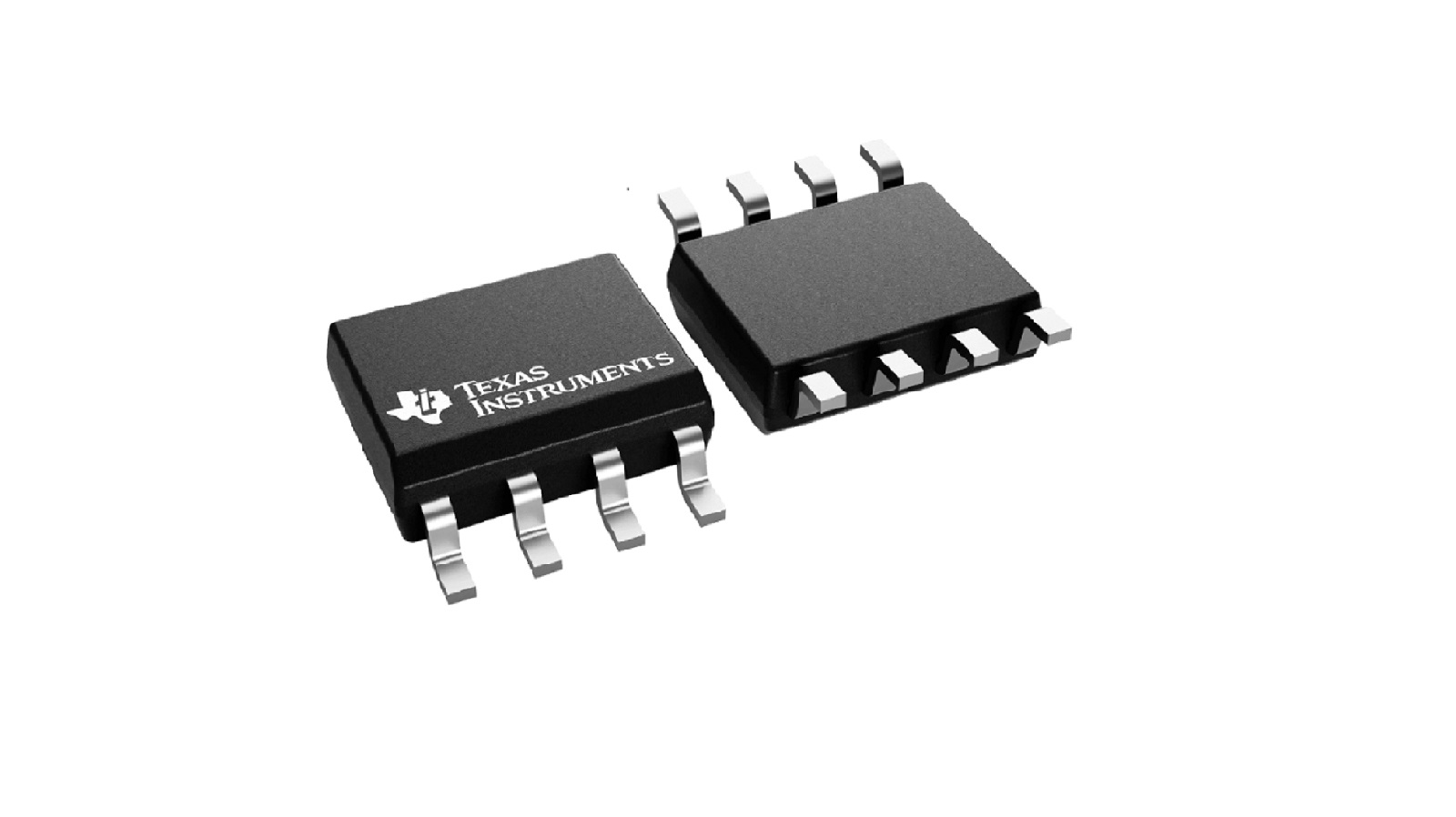
Description: Small in shape, with small-pitch pin layout.
Sizes: Generally, 3x3mm, 5x5mm, 7x7mm.
Number of Pins: Generally in the range of 8 to 48.
Applications: Suitable for medium-scale integrated circuits.
Through-Hole Technology (THT)
The Through-hole packages have pins that pass through pre-drilled holes in the PCB and soldered on the other side for making reliable mechanical and electrical connections.
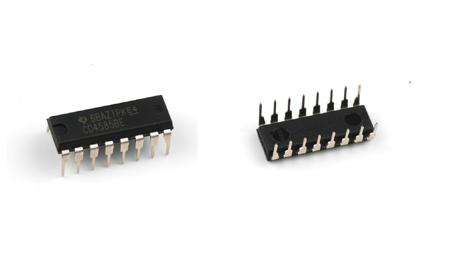
Dual In-line Package (DIP)
Description: Two parallel rows of pins in a rectangular package.
Sizes: Generally 7.62mm pitch
Number of Pins: 4 to 64.
Applications: Extremely broad applications in consumer electronics, industrial machinery, and automotive.
Single In-line Pin Package (SIP)
Description: One row of pins issued vertically along the edge.
Common Variants: SIP, SSIP, HSIP.
Applications: Network resistors, RAM chips.
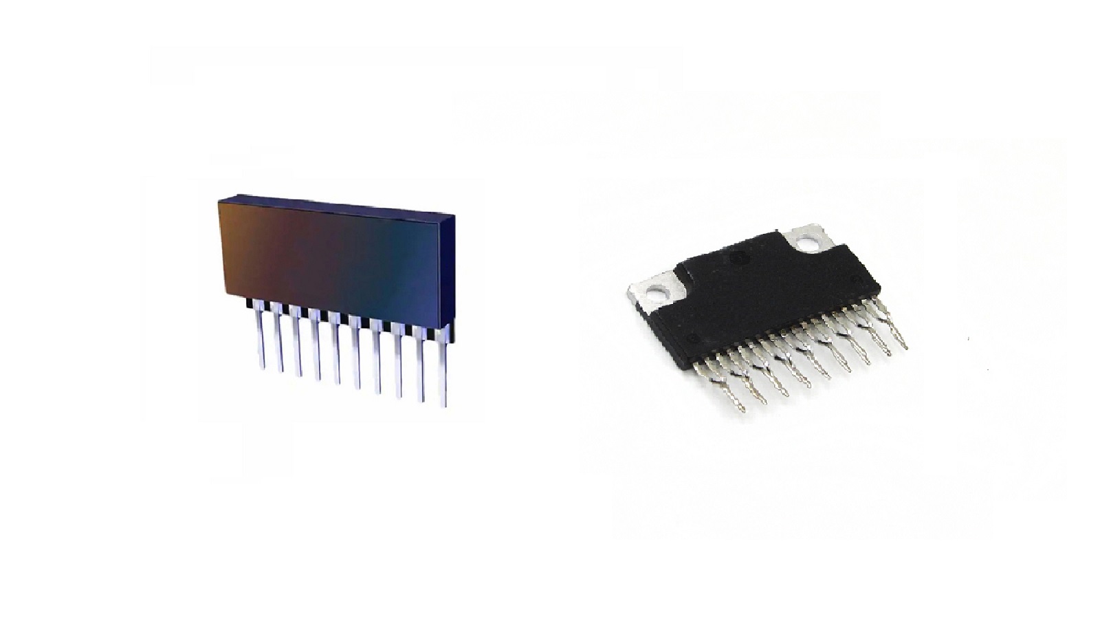
Zig-Zag In-line Package (ZIP)
Description: SIP-like package with zigzag folded pins.
Common Variants: ZIP, SZIP.
Applications: Memory modules, custom IC applications.
Other Types of Packages
Chip-on-Board (COB)
Description: Chip is directly mounted on the PCB.
Applications: Used in compact equipment and products where high integration is required.
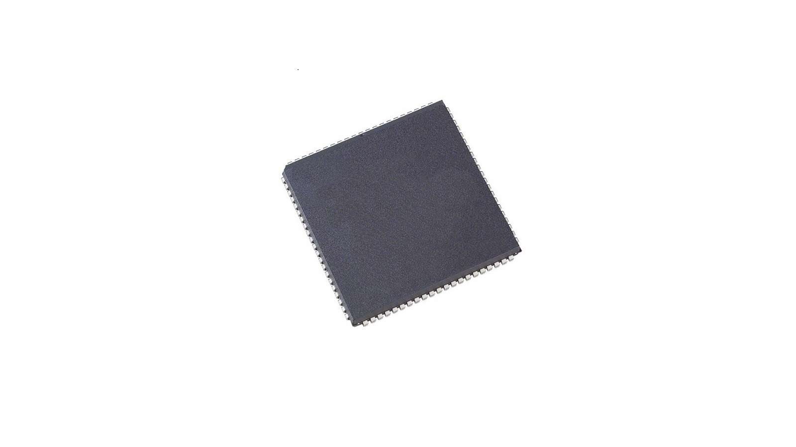
Plastic Leaded Chip Carrier (PLCC)
Description: Very integrated digital circuits.
Sizes: About 20x20mm.
Pin Count: Varies between 20 and 84.
Applications: Smaller designs for high-density PCBs.
Information about Packaging of ICs
Some of the key information usually packaged in IC packages includes:
Type and Size of Package: Type of package and its measurement in length, width, and height.
Pin Configuration and Pin Count: The configuration of pins and number traces the component functionality and type of interfacing.
Type of Material Used: This impacts mechanical strength and also affects the thermal performance of the package.
Pad Information: Information like pad location, shape, and size for soldering is depicted.
Thermal Management: Parameters for heat dissipation so that operational temperature is maintained.
Package Identification: Manufacturer's logo, model number, date code for traceability.
Pin Function: Pin functions are described for correct circuit connections.
Environmental Adaptability: The various environments the package can withstand, such as waterproof and dustproof.
Standards for IC Packaging
IPC 7351: Defines the physical size, pin layout, and pad design of standard SMD component packages.
ANSI Y32.2-1975: Lists the symbols of various electrical and electronic components.
ISO 10303-21: STEP file format for 3D CAD model standardisation.
Guidelines to Design IC Package
Package Dimension: The size and shape of the package must be according to a particular component specification.
Pin Placement: No two pins should be overlapped and collocated, the spacing between every two pins should be large enough for easy soldering.
Pad Design: Proper pad size and shape ensures welding quality and reliability.
Thermal Management: Provide appropriate heat sink structures for the high-power component.
Symbol Marking: Proper symbolic marking helps to make identification and design easy.
3D Modeling: Allows for PCB modeling and collision detection.
Prohibited Areas: Allocate enough prohibited areas in every PCB to avoid component collisions.
Manufacturability: Pay attention to limitations with regard to manufacturing and assembly during design.
Choosing the Right Package of IC
Variety of IC Packages Available:
Surface Mount Technology (SMT) finds applications in small-sized electronic equipment such as smartphones, tablets.
Through-Hole Technology (THT) is best fitted for large electrical and mechanical connections, such as in systems for industrial control.
SiP stands for System-in-Package, which integrates many functional modules for higher integration and performance.
BGA, or Ball Grid Array, is a surface-mount package with a high-density solder ball array, fitted for high-performance applications.
Determination of Functional and Performance Requirements
The signal integrity is very important when there is a high-frequency or high-speed signal; one should choose a package which has superior signal integrity.
Size Restrictions: Match the size of the package with PCB layout to avoid installation problems.
Cooling and Thermal Management
Heat Dissipation: Choose appropriate packages with good heat-dissipation designs for high-power ICs.
Layout and Routing
Pinout Matching: Match your package to your layout to ensure good signal integrity and electrical interfaces.
Cost and Supply Chain Availability
Balancing Cost and Performance: Make sure the chosen package fits within your project's requirement of budget and timeline.
Conclusion
Understanding IC packaging is a stepping stone to effectively designing the PCB. If you consider the type of package, size, pin layout, thermal management, and constraints at manufacture, you can correctly integrate components into a circuit. Being informed about the latest industry trends and standards will help you in making optimum decisions that will enhance performance and dependability for your electronic products.
Be it the design for an industrial control system, automotive electronics, or any other application requiring difficult conditions, it is clear that IC packages offer solutions that really combine reliability with ease of operation. With the appropriate selection of an IC package, you can make a huge difference to the success of your PCB design project.
Hot Tags:
Contact us

If you can't find what you're looking for, please contact us.
Article
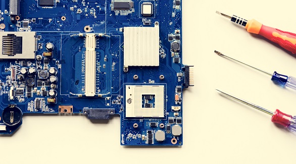
PCBX offers reliable, low-cost, low-volume PCB assembly with custom specs, superior quality control, and excellent customer support, ensuring high customer satisfaction.
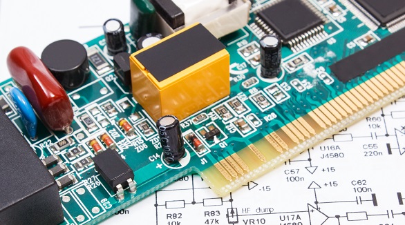
Turnkey PCB assembly means the provider handles everything from component procurement to manufacturing and assembly. PCBX, serving 80+ countries, offers reliable, cost-saving, one-stop solutions with faster lead times and consistent quality.
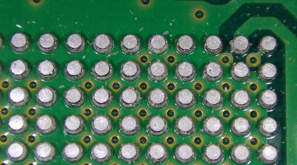
In the late 1980s, when electronics began to shrink, BGA packaging was developed to integrate more connections within a given area. Today, BGA is widely used with high-connection chips—processors being a good example. BGA uses solder balls at the bottom of the chip to connect it to the circuit board. It provides high density along with good heat dissipation and fast signal transmission, one of the main reasons it is ideal for modern electronics. However, it requires precise techniques of soldering in BGA manufacturing.