- Products & Capabilities

- About
- Resources
Comprehensive Guide to PCB Panel Creation


PCB panelization consolidates multiple PCBs into a larger board, improving manufacturing efficiency and reducing waste. Techniques include V-scoring and tab-routing. Proper design enhances assembly, testing, and cost-effectiveness.
Panel creation, more appropriately called panelization of a Printed Circuit Board, is the process of compiling several individual PCB designs into one larger board commonly known as a panel. It is more than just space-saving - an approach aimed at improving manufacturing efficiency and therefore reducing material waste to reduce production cost. The following tutorial will help a person-whether a learner or an experienced one-understand the creation of a PCB panel, from basic concepts and specific types of panels to the techniques involved, in order to get a perfect sense of the concept.
Need for the Creation of PCB Panel
Why Panelization?
The main problem-or better said-the motive for creating PCB panel creation is to make the process of manufacturing easier. Placing several smaller PCBs together into one big panel facilitates-and saves time for-the manufacturer. Advantages involved include:
Improved Manufacturing Yield: A single large panel is much more convenient to handle in a manufacturing process than many small boards.
Economic Advantages: Material wastage is minimized due to the fact that unused space between individual PCBs in a panel will be at a minimum.
Easy Assembly and Testing: This makes it easier in SMT assembly and testing since multiple boards are processed in one run.
Types of PCB Panels
Common Panel Types
Different panelization techniques fit various requirements and PCB designs. Among the major types of panels are:
V-scoring/V-cut/V-groove:
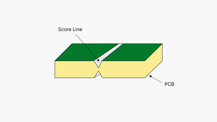
Description: A 'V' groove between boards, the method gives good results when the board snaps off easily. It could be appropriate for PCBs whose edges are just plain and straight.
Application: Suitable for rectangular-shaped PCBs and is done on a V-cut machine. A cut is made through the full board continuously, so this technique can also be used for volume production.
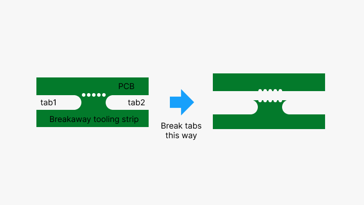
Routing Slot/Milling Slot + Tab (Tab-routing):
Description: This is a process of milling slot in between PCBs while leaving some tabs to hold the PCB structurally. There are two kinds of tab-routing:
Tabs with perforations/mouse bites that can be easily snapped.
Solid tabs that need to be cut.
Application: This method can be applied to the PCBs, which are of irregular shapes and sizes since the tabs will act like supporting edges, which can be easily snapped off when needed.
Combination of V-scoring and Tab-routing:
Description: This method shall be applied when a panel needs both methods for its completion owing to several design needs. For instance, V-scoring for the edges, which are straight while for other irregular shapes, tabs may be required.
Rules and Tips to Carry Out Efficient Panel Design
Considerations During Design
Some of the key design rules to consider when ensuring efficiency and quality in PCB panelization include:
Panel Shape: The design should aim for a square or rectangle for convenience in handling and space maximization.
Closed-loop Outer Frame: Ensuring that the panel retains its shape during a time-consuming manufacturing process.
Components Placement: Large or protruding components should not be put near the connection point between the panel frame and the individual PCBs.
Fiducial Marks: The panel should feature at least four fiducial holes, situated in its corners. These are for alignment purposes during the manufacturing process. The location must be accurate, and the sidewalls must be smooth to avoid structural weakness.
Fiducial Points: There must be an area devoid of solder with a diameter greater than 1.5mm around each fiducial mark for viewing purposes.
Mechanical Processing Techniques
Scoring and Milling
Multiplier Panel Scored:
X Spacing: No spacing between PCBs. Where space is needed, a minimum 5.0mm spacing must be used.
X Traces and Copper Areas: All traces and copper areas must be at least 500µm from the scoring edge.
X Panel Thickness: For rigidity, it is advisable to use scoring on panels with the minimum thickness of 1mm.
Multiplier Panel Milled:
X Spacing: Leave a 2.0mm gap between PCBs.
Bridges: If left undefined, the manufactures will place them optimally-usually 1.0-1.5mm wide.
Traces and Copper Areas: Keep 200µm minimum distance from milling edge.
Mixed Multiplier Panels:
Description: Place various different PCB layouts together into one panel.
Contours and Traces: Same spacing (0.0mm for scoring, 2.0mm for milling).
Stability: Leave enough room for panel stability.
Combining Techniques: Scoring and Milling
Usage and Recommendations
Combination of scoring and milling techniques can provide solutions for complicated panel designs:
Calculation of Spacing: Keep the spacing between scored parts as 0.0mm and that between milled parts as 2.0mm.
Spacing on Edges: Keep all traces and copper areas at least 500µm from the scoring edge and 200µm from the milling edge.
Tool Issues to Consider: It is best to avoid milling straight down a scoring line due to chip formation issues during manufacturing.
X-out Management and Customer Involvement
X-out Handling:
Standard Practice: A defective PCB (determined through E-test) is left on the panel but is X-ed out.
Customer Options: Customers, during the ordering process, have an option to NOT allow this process to ensure no marked defective PCBs are delivered.
Customer-Driven Design:
Panel Data: Customers may supply their panel configuration or use manufacturers' online tools for exacting panel assembly.
Configurator Tools: These are the tools that give a preview about the design of a panel to facilitate the panelization process. This is done so in order to ensure customer satisfaction.
Conclusion
PCB panel creation is an essential part of modern electronic manufacturing. It is an amalgamation of art and science put together with an objective of enhancing efficiency that would reduce the cost and best methodology of assembly. Understanding various methods and best practices for panelization would ensure high-quality, cost-effective PCBs both by designers and manufacturers. You will become proficient in the creation of a panel for the PCB, taking into account the types of panels that may be produced, the mechanical processing methods involved, and some of the essential design rules, thus getting the many benefits accruable from using them in manufacturing.
Hot Tags:

Contact us

If you can't find what you're looking for, please contact us.
Article
Solder masks protect PCBs from environmental damage and electrical shorts, enhancing reliability and aesthetics. The application is complex, requiring professional fabrication to ensure quality and compliance with regulations.
 2024/08/20
Plated-through slots (PTS) in PCBs are copper-plated apertures for electrical connectivity, offering space optimization, reduced soldering voids, and improved surface use.
2024/08/06
The article is developed concerning the breakthrough of integrated circuits and the need for custom PCBs in some electronic products. It enumerates ten golden rules in conducting PCB layout design and manufacturing: grid selection, routing, power layers, component placement, panel duplication, component value combination, frequent DRC, flexible silkscreen use, decoupling capacitors, and pre-production parameter checks. These rules provide for the optimum design and manufacturing of a PCB.
2024/07/25