Controlled Impedance in PCB Design
Controlled impedance is crucial in modern PCBs, ensuring signal integrity through precise trace and material design, essential for high-speed applications.
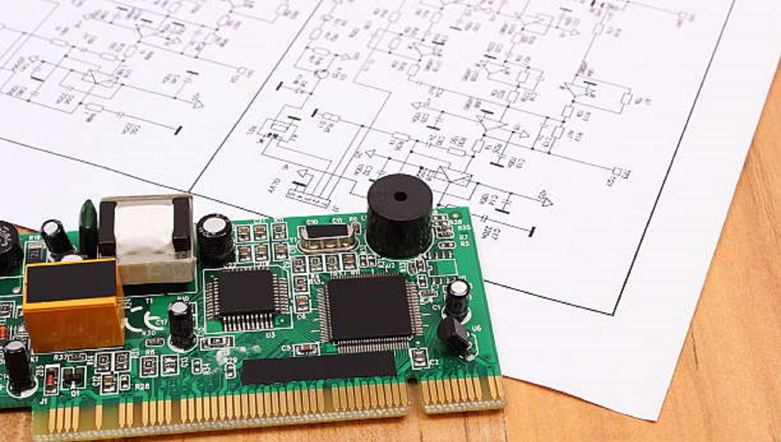
The printed circuit boards, or PCBs, form the very backbone of modern electronic devices by providing a framework that is so critical in allowing complex communication between different components. While technology pushes the boundaries even further with regard to size, speed, and functionality, so have design and manufacturing of PCBs become increasingly sophisticated. Among many techniques being utilized to make sure that the PCBs can meet these high standards, controlled impedance is a key factor for success. In this piece, we’ll explore what controlled impedance is, why it’s crucial, and how it is reliably achieved in PCB design and manufacturing.
Controlled impedance refers to the deliberate regulation of the electrical impedance within the signal traces on a PCB. These signal traces function as the pathways for electronic signals, which are essential for the device to perform its intended operations. Unlike the simple DC paths, these traces will carry high-speed, high-frequency AC signals. The impedance here is a complex combination of resistance, inductance, and capacitance that has significant implications on how the signal will travel across the PCB.
Why impedance control? The path needs to be without distortion and correctly timed throughout its journey of travel. Impedance is determined depending on the trace dimensions, substrate materials, and the dielectric constant. The aim here will be to make sure the traces remain uniform, so the signal transmits with integrity without reflections or degradations that would affect performance.

Why is Controlled Impedance Important?
Impedance control is vital to signal integrity, especially in modern demands for speed and efficiency in electronic devices. Poorly controlled impedance gives rise to reflections-the jumping of the signal back toward the source-or attenuation, where the signal attenuates while navigating through the PCB. Both of these scenarios will work to compromise functionality and lead to possible failures.
In RF, telecommunication, or high-speed digital signal applications, the accuracy of signal transmission is critical. Smaller PCBs require more intricate designs to fit in more functionality within a reduced space, and hence their tolerances are smaller, which again requires precision in impedance control. In such devices, even a minute change in impedance can considerably alter performance, and hence, controlled impedance is not only useful but indispensable.
How to achieve Controlled Impedance
It is attained by paying great attention to a number of design features. Usually, close interaction between designers and producers is required for achieving controlled impedance. The following are some of the main ways it is achieved.
Trace Dimensions: Simple changes make all the difference. Width, thickness, and spacing are critical. Wide traces have low impedance, while narrow traces have high impedance. A designer needs to calculate very accurate dimensions in order to reach the required impedance.
Material Selection: The PCB substrate material’s dielectric properties play a crucial role, affecting how signals propagate across the board. Different materials can drastically influence impedance, so choosing the correct material is imperative to meet design specifications.
Layer Configuration and Stackup: In multi-layer PCBs, the layer stackup can have a great impact on impedance. For that, configurations such as microstrip and stripline designs may be utilized to effectively manage impedance. A microstrip places the signal trace on an external PCB layer, with a reference plane below, while a stripline positions the trace between two reference planes within the PCB.
Simulation and Testing: Before manufacturing, designers make use of advanced simulation tools to predict impedance based on the proposed designs; this stage allows for adjustments in the design parameters using physical conformance to expected electrical behaviors.
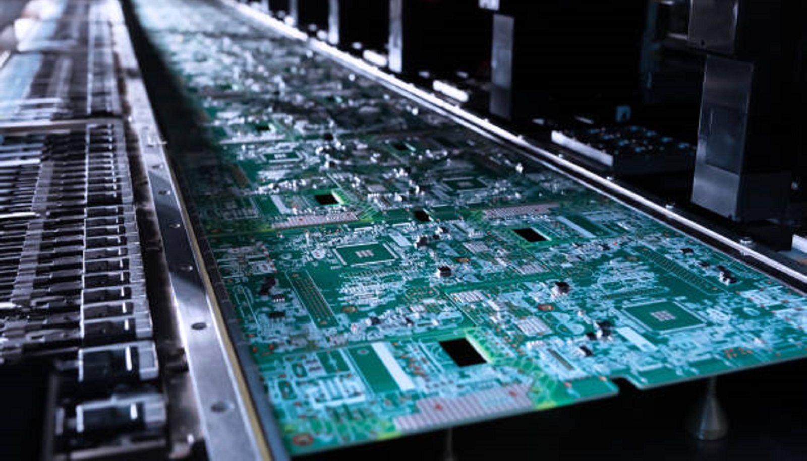
Precision Manufacturing: After design, precision fabrication techniques ensure that the etching and layering of the traces of a PCB are according to exact specifications. Collaboration between designers and manufacturers is important. The manufacturer must engage in techniques that precisely control the trace dimensions during fabrication, including material characteristics.
Collaborative Development and Expertise
Controlled impedance implementation requires an integrated approach wherein design ingenuity meets manufacturing precision. That is a synergistic realm wherein service providers like PCBX become invaluable partners. We provide experienced guidance both in the design and production stages to make sure that your PCBs perform optimally.
We use short-run PCB services for verification and refinement of the PCB design in realistic conditions. Such a process identifies the best material, trace configuration, and layer stackup for the required impedance control, thus making quick changes as iterative feedback is obtained.

It is not just a part of PCB design; rather, it's an enabler for performance and reliability in advanced electronic devices. The landscape keeps on evolving in the field of high-speed, high-frequency applications, and hence controlled impedance will no longer be optional but rather an enabler of success.
At PCBX, we are committed to helping our customers meet their controlled impedance needs by providing the required experience and knowledge to address these increasingly complex issues. Let's make sure we improve the state-of-the-art technology demands in your gadgets while having signal integrity of immaculate standards on their printed circuit boards. Feel assured with impedance-controlled impedance and preservation of your signal fidelities with your product, staying one notch above others within this electronics field. From design optimizations down to material selection and precision manufacturing, our approach to controlled impedance is all about the delivery of the highest standards of performance for your projects.
Hot Tags:
Contact us

If you can't find what you're looking for, please contact us.
Article

Castellated pads in PCB design facilitate easy board-to-board connections, enhancing miniaturization, assembly, solder quality, and flexibility for compact modules.

Capacitors are crucial in PCB design for filtering and timing. Correct polarity in electrolytic and tantalum types prevents malfunctions and ensures reliability.

Designing PCBs for IoT demands innovation to tackle space, power, connectivity, and security challenges, ensuring robust, efficient, cost-effective devices that meet modern technological demands.
