- Products & Capabilities

- Simulation Design & EDA

- About
- Resources
Dendrite Growth and Contamination in PCBs


Preventing dendrite growth and contamination in PCBs is vital for reliability; effective testing and controls ensure longevity and performance in electronics.
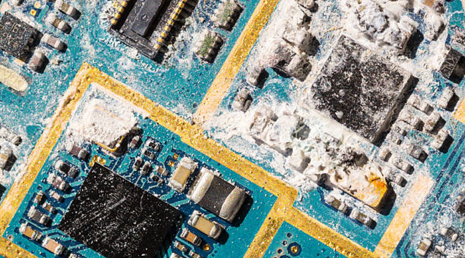
Among these different challenges in the competitive electronic manufacturing scenario, performance and reliability of PCBs can be maintained by preventing dendrite growth and contamination, which are the hidden threats to severe malfunction and circuit failure. These phenomena, though usually hidden, call for adequate consideration and proactive management to ensure longevity and effectiveness in electronic devices. The development of dendrite growth and contamination in PCBs, their causes, effects, and mitigation methods are discussed, along with effective testing. What is Dendrite Growth? Dendrite growth in printed circuit boards refers to the generation of metallic filaments that appear between conductive paths. Most of the time, it appears due to electrochemical migration under conditions of high humidity, voltage bias, and ionic contamination. With this process ongoing, the dendrites are usually made of metals like silver, tin, and copper that can eventually form unintended conductive paths, which cause short circuits and lead to failure. Even though less frequent in nickel, cases have been noted in specified conditions: upon exposure to moisture and sulfuric acid contamination (H2SO4) derived from manufacturing processes.
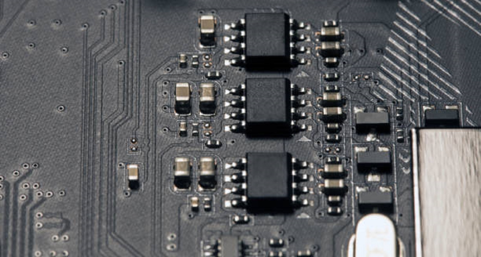
Dendrite Growth Factors
Moisture and Relative Humidity: Water is a medium for metal ions to dissolve in and migrate. Higher temperatures can sometimes decrease the humidity at the surface, reducing the dendrite growth rate. On the other hand, high condensing conditions can drastically enhance the process.
Voltage Bias: The potential difference between conducting elements can act as the driving force for metal ions to migrate and deposit as dendrites.
Ionic Contamination: Residues, usually from manufacturing processes, increase conductivity on the PCB surface, allowing electrochemical reactions to take place.
Effects of Dendrite Growth and Ionic Residues
The growth of dendrites and ionic contamination can have serious implications for the performance of a PCB, including:
Corrosion: Ionic residues catalyze corrosion processes, shortening the lifespan of a PCB. This rapid deterioration is particularly worrying in areas where moisture and contaminants combine to form rust and oxide layers.
Short Circuits: Dendrites form bridges across isolated conductive paths, which result in short circuits and render the whole circuit unusable.
Electrochemical Migration: In regard to dendrite formation, it is where dendrites redirect the flow of current across dielectric materials, resulting in intermittent or complete failures.
Cleanliness and Contamination Testing
These two challenges of dendrite growth and contamination need specific testing measures in order to proactively address the problem. Contamination testing allows for the identification and management of ionic residues that could lead to the jeopardy of PCB integrity.
Testing Techniques
Resistivity Testing: This is a simple test that gives the initial indication of board cleanliness based on impedance measured during the cleaning process of the PCB.
ROSE Test: This traditionally used test is one of the various techniques for measuring conductivity of the solvent extract from PCB, thus offering a quantitative measure of overall ionic content in it.
Modified ROSE Test: In addition to the normal ROSE test, there exists a Modified ROSE Test that incorporates thermal extraction methods, adding even greater insights into the abilities of transient environmental conditions to act upon ionic contamination.
IC Testing: With the use of IC testing, detailed analysis identifies certain ionic species and their overall concentration. Chromatography applied in this type of testing separates ions and thus provides information on those contaminants that make PCB unreliable.
Importance of Dendrite Growth and Ionic Contamination Analysis
Recognizing and addressing contamination is important, as about 25% of PCB failures are related to ionic impurities. Efficient testing enables the manufacturer to find the source of contamination and apply corrective measures that minimize the chances of failure and financial loss due to product recalls or warranty claims.
Preventive Measures and Industry Standards
Dendrite growth and contamination pose a number of risks that can only be minimized with appropriate preventive strategies:
Design Considerations: The right spacing between the conductor paths and applying quality conformal coatings will decrease the risk of electrochemical migration.
Environmental Controls: Controlling operating and storage environmental humidity and temperature will, in turn, reduce conditions that would facilitate the growth of dendrites through electrochemical migration.
Thorough Cleaning Processes: Advanced cleaning procedures integral in manufacturing help take care of ionic residues, thus ensuring board cleanliness.
IPC Standards: Following the respective industry guidelines, such as IPC-TM-650, which detail the test methods for ionic testing, helps to maintain the high standards of cleanliness on PCBs.
Dendrite growth and contamination pose serious challenges in the manufacturing and operation of PCBs. These phenomena can seriously affect the reliability and performance of electronic devices if not addressed proactively. This could greatly reduce the associated risks on such issues by the manufacturers through comprehensive testing, besides adherence to rigorous environmental and cleaning standards. Such sophisticated testing methods like ion chromatography and ROSE testing provide valuable insights to manufacturers to refine their processes further in improving product quality. At PCBX, we are determined to provide with solutions and analyses that will offer protection to your electronic components with a view of ensuring their reliability for today's and tomorrow's arduous applications. In this way, dendrite growth and contamination can be maintained within threshold ranges by continuous innovative approaches and strict adherence to best practices in order to afford resilient and reliable electronic devices.
Hot Tags:

Contact us

If you can't find what you're looking for, please contact us.
Article
PCB encapsulation offers vital protection against environmental, mechanical, and security threats, ensuring the reliability and longevity of modern electronic devices.
 2025/01/17
PCB insertion loss is crucial to managing signal attenuation in high-frequency designs, affected by materials, path length, and connectors—optimized through strategic design measures.
2025/01/16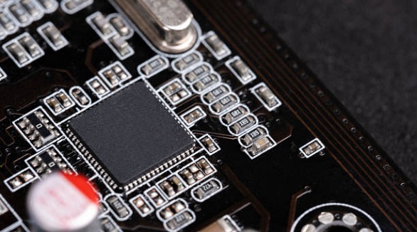
Embedded PCB components enhance space efficiency, reliability, and performance, driving innovation in compact electronics for consumer, automotive, and medical applications.
2024/12/26