- Products & Capabilities

- Simulation Design & EDA

- About
- Resources
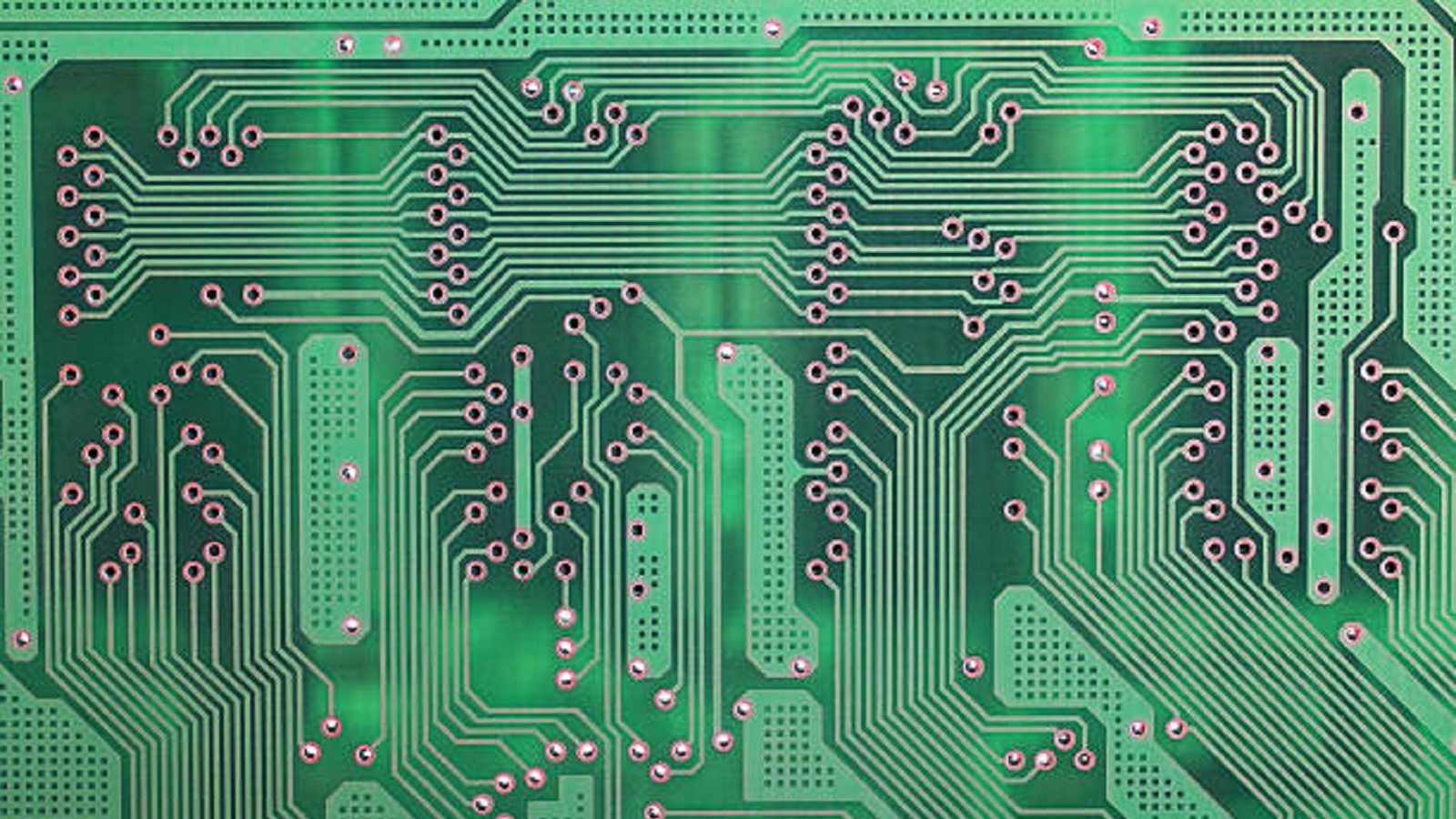
Designing PCB Safety Spacing


PCB design hinges on safe spacing for reliability; it prevents short circuits and ensures durability, addressing both electrical and non-electrical factors.
In the world of electronics, printed circuit board design acts as the backbone for a variety of devices, from simple gadgets to advanced technological systems. With increasing complexity and miniaturization of components, safety and reliability become prime concerns for PCBs. One of the critical aspects of achieving this involves careful consideration of PCB safety spacing, focusing both on electrical and non-electrical characteristics. This article describes how to design spacing for safety in a PCB and provides best practices for optimizing both categories.
Importance of Safety Spacing in PCB
Spacing for safety in the design of PCBs is important for several reasons, including the following:
Prevention of Short Circuits and Arcing: It prevents short circuits and arcing. Appropriate spacing avoids unintended electrical connectors or conductive pathways that can lead to short circuits, which may further damage components or the whole device.
Reliability across Environments: PCBs work in various environmental conditions, such as high humidity, temperature fluctuations, and pollution. Enough safety spacing ensures continued performance and reliability across these conditions.
Compliance with Industry Standards: Following the safety standards set by IPC, for example, means that the design is robust, with a reduced chance of field failures and safety to the consumer.

Categories of PCB Safety Spacing
The safety spacing of a PCB can be divided into two major classes: electrical-related safety spacing and non-electrical-related safety spacing. Both are important for the overall integrity and functionality of a PCB.
Electrical-Related Safety Spacing
Electrical safety spacing is generally related to proper alignment and spacing of conductive elements to avoid electrical failures. Following are some key areas of attention: -
Wire Spacing
The spacing between conductive wire traces on a PCB is critical in preventing crosstalk of signals and short circuits. In most cases, the minimum spacing should be 4 mils for mainstream PCB manufacturers; however, it is advisable to keep a spacing of 10 mils or more, which provides a cushion for imperfections in manufacturing and variations in the operating environment.
Pad Aperture and Pad Width
Pads attach parts to the PCB, and a fabrication tolerance and performance of parts need to be included in their spacing. All the mechanical drilling should be no smaller than 0.2mm minimum diameter while laser drilling allows more refined diameters down to 4 mils. Recommended pad width should be at least 0.2mm to provide solid structure and good connectivity.
Pad to Pad Spacing
Pad spacing of not less than 0.2mm would be adequate to prevent solder bridging for clean component installation. Proper spacing allows automated processes for assembly with reduced electrical shorts.
Copper and Edge of the Board Spacing
Routings of copper traces at the edge of the PCB are carefully done to avoid their exposure to physical damage and making an electrical connection to some other external elements. Good practice would be to make spacings of at least 0.3mm minimum and for extensive copper areas a retreat from the edge of at least 20 mils. This retraction acts to reduce the risk of curling and accidental exposure.
Non-Electrical-Related Safety Spacing
Safety non-electrical spacing ensures physical and mechanical integrity of the printed circuit board to accommodate conditions of assemblies and operations.
Character Width, Height, and Spacing
Labels and instructions are included on PCBs using text and silkscreens. Character should be clear and legible with 0.22mm line width, the full character width of 1.0mm and height of 1.2mm. A spacing of at least 0.2mm between characters for readability without overlap during the manufacturing process.
Via to Via Spacing
Vias allow signals to move between layers in a PCB. For structure and signal integrity, keep the via spacing above 8 mils. This allowance is so that thermal stress and compromise do not occur in soldering.
Silk Screen to Pad Distance
Silk-screen markings are never to impair solderability. A separation between components' markings of about 8 mils allows not experiencing problems in this stage. Still, some compact design could have smaller dimensions even to 4 mills and can be feasible by only keeping in thought avoiding overlaying soldering pad spaces.
Mechanical 3D Height and Horizontal Spacing
In designing the PCBs, consider space above and around components to avoid conflict with any enclosures or other mechanical parts. Sufficient spacing is highly important not only for proper component fitment but also for allowing proper airflow for heat dissipation.
Safety and Success Considerations
Designing PCBs that handle both electrical and non-electrical safety spacing calls for great detail in meeting the requirements and constraints of your project. Below go some tips for success:
Simulation and Testing
Use design simulation tools to model electrical behavior against a variety of conditions. The simulations can spot failure points that may occur, give spacing to accommodate changes in such failures, and help optimize a design prior to creating a physical prototype.
Iterative Prototyping
Building and testing multiple prototype iterations can reveal issues not visible in simulations, allowing designers to refine safety spacing based on empirical data.
Standard Compliance
Familiarize yourself with industry standards (e.g., IPC guidelines) to incorporate best practices and ensure design compliance. This adherence not only facilitates manufacturing but also helps in meeting regulatory requirements.
Component Selection and Placement
Choose components with care, considering space and interaction requirements. Proper placement can have a huge effect on safety spacing, both electrically and mechanically.
Proper PCB safety spacing is what forms the bases for efficient, reliable, and safe electronic equipment development. Being fully cognizant and applying all those principles of both electrical and non-electrical spacing, the designer could further improve on performance, longevity, while keeping up with the steps in industry standards. All in all, holistic PCB spacing for innovation and excellence in electronics engineering requires not only great creativity but an approach oriented toward interdisciplinary harmony.
Hot Tags:

Contact us

If you can't find what you're looking for, please contact us.
Article

FR4 permittivity affects PCB signal speed and impedance. It's crucial for design, requiring careful management in high-frequency applications for reliability.
 2024/12/16
DFM ensures cost-effective PCB design by optimizing size, layers, materials, and components, focusing on manufacturability, reliability, and process efficiency.
2024/10/30
Tab routing enhances PCB production efficiency and quality, ideal for complex shapes. It offers cost-effectiveness, flexibility, and protection, crucial for high-precision designs and panelization.
2024/10/23