Edge Connector Bevelling in PCB Design
Edge connector bevelling enhances PCB durability and reliable connections, vital for frequent usage and secure engagements, with limitations primarily in plating.
In the broad field of PCB design, attention to minute details can make a great deal of difference in the long life and performance of an electronic system. Such a minute detail is edge connector bevelling, which is applied to improve the interaction between a PCB and its corresponding connectors. This article gives an overview of edge connector bevelling, with an emphasis on the critical role, benefits, and limitations of technology in PCB applications.
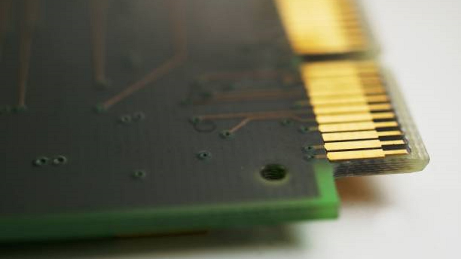
Edge connector beveling is the process that provides an angled edge for a PCB where it would interface with connectors, usually card edge connectors. As a process, this occurs right after solder masking but before surface finishing to ensure ease in inserting the PCB into connectors and vice versa. Angles that are usually provided range from 30 to 45 degrees, making this engagement smooth and reliable.

Why Is Edge Connector Bevelling Necessary?
The frequent plugging and unplugging of PCBs, as is common in many electronic applications, require contact points that are durable and reliable. Edge connector bevelling plays an important role regarding:
Ease of Insertion
Bevelling causes the edges to slope, which allows the PCB to smoothly enter connectors with reduced insertion force, hence minimizing any possible damage. It thus makes the insertion easier, particularly for applications requiring frequent removal of the board for testing and upgrades.
Reliability of Contacts
Beveled edges ensure proper and consistent alignment and engagement of contact pads with connector pins. Very stable electrical connections with minimal risk of intermittent faults result.
Reduced Wear
The chamfered edge reduces the friction between the PCB and connector during insertion and removal, reducing the wear on both components. Long-term performance is very critical in systems with high-frequency connect-disconnect cycles.
Improved Durability
Bevelling reduces stress concentration, thereby giving additional strength to the structural integrity of the edges of the PCB and helping to avoid crack or delamination during operation.
Role of Gold Plating
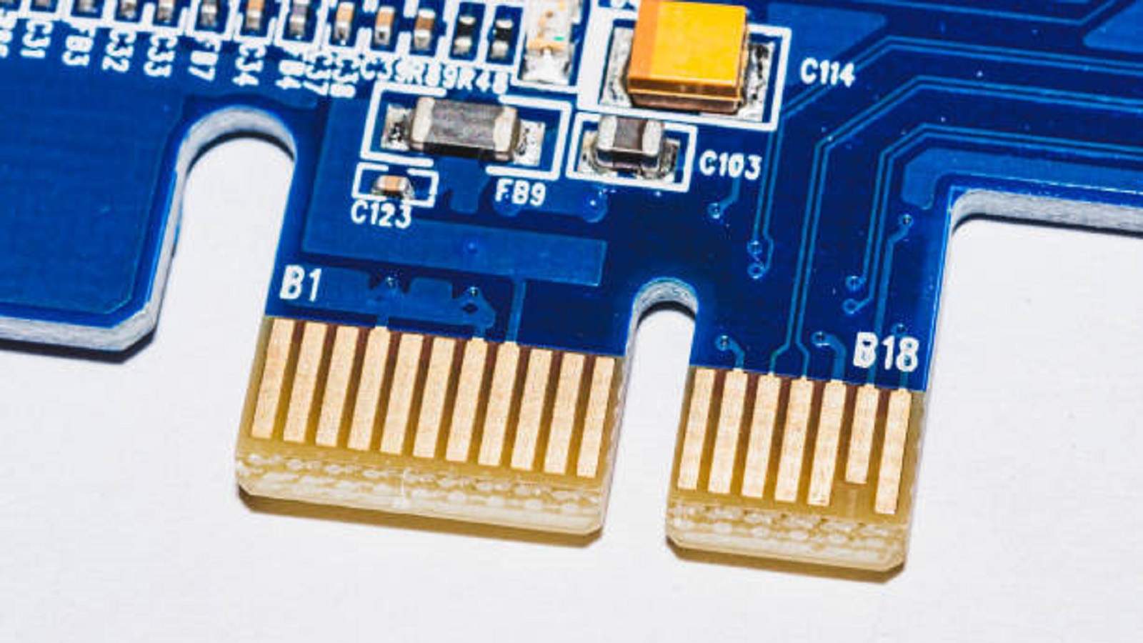
Gold is one of the metals generally used on the contact edges or "gold fingers" of PCBs because of its high electrical conductivity and resistance to corrosion. Though it is a bit expensive compared to alternatives like copper, gold plating provides the assurance in durability and reliability of edge connections of the PCB for:
Conductivity and Corrosion Resistance
Gold's excellent conductivity allows minimal resistance along the contact path to maintain signal integrity. It resists oxidation, thus maintaining the quality of connections with time.
Alloying Benefits
In practice, gold is usually combined with metals such as cobalt or nickel to provide more resistance to wear and further improve the life cycle of edge connectors.
Chamfering within Edge Connector Bevelling
Chamfering provides for a beveled edge that allows for smooth mating with connectors. The designer needs to ensure that the chamfer angle and tolerances are according to the specifications of the connector manufacturers. These specifications allow the PCB fabricator to perform the bevelling process accurately to enable secure and efficient installation into standard interfaces.
Limitations of Edge Connector Bevelling
Even though bevelling has its advantages, the process has some limitations:
Plating Requirements
The gold finger method requires the plating pads to be at the edge of the PCB. This calls for electroplating, which can be problematic in manufacturing if longer gold fingers are needed.
Restrictions on Internal Layers
To avoid exposure during bevelling, the internal layers of a PCB should not have copper near the edges. Exposed copper will create reliability problems if not managed appropriately.
Dimensional Constraints
When plating both sides of a PCB, the separation between upper and lower layers should not exceed certain limits (typically around 150mm), and gold finger lengths should remain within 40mm to maintain manufacturing precision.
Impact on Functionality
The change in pad length due to manufacturing tolerances may affect connectivity, hence engineering should be precise at the design stage.
Applications of Gold Fingers
Gold fingers are major connective regions that connect circuit boards in a system. Their high electrical conductivity ensures that there is effective communication between the components. The key applications include:
Installation of Components
Beveled gold fingers allow easy installation of additional components or upgrading to a PCB.
Interconnection Points: Gold fingers also provide interfaces between various components and the motherboard that route signals through slots such as PCI, AGP, and ISA.
External Connections: The gold fingers offer heavy-duty external connections, making communication between machinery and control systems quite reliable.

Bevelling in an edge connector is a major stage in the design of the PCB, which enables the accurate shaping of the contact edges to establish a secure connection with other components. It improves insertion ease, contact reliability, and protection against wear, hence contributing much to the life and performance of electronic assemblies. Limitations aside, be it for manufacturing constraints or material requirements, advantages of bevelling-most with gold plating-reiterate that it is a key component of constructing robust and reliable electronic systems. Bevelling will continue to be very important, both for designers and manufacturers of PCBs, as technology advances and efficiency at edge connector solutions is an ever-growing need.
Hot Tags:
Contact us

If you can't find what you're looking for, please contact us.
Article

FR4 permittivity affects PCB signal speed and impedance. It's crucial for design, requiring careful management in high-frequency applications for reliability.

Designing PCBs for IoT demands innovation to tackle space, power, connectivity, and security challenges, ensuring robust, efficient, cost-effective devices that meet modern technological demands.

IC packaging is essential in electronics for protecting components, providing electrical connections, and managing heat. This tutorial explores its complexities, including its importance, various types like SMD, QFP, and BGA, and considerations for choosing the right package for specific applications. Proper IC packaging enhances PCB performance and reliability.
