Functional Testing in PCB Assembly
Functional testing verifies PCB functionality in simulated environments, enhancing quality and reliability, detecting faults, ensuring performance, and cost efficiency.
Functional testing in the complex world of PCB assembly represents the last check that ensures the operational integrity of a PCB. It is the last stage that gives assurance an assembly is defect-free and meets the specified performance criteria before declaring a board ready for deployment. This process simulates the intended electrical environment of the PCB in order to test and verify the performance of all components within their operational context. This article from PCBX discusses several aspects of functional testing in PCB assembly, regarding its advantages, procedure, planning, and key considerations when choosing a manufacturer.
Advantages of Functional Testing
Functional testing carried out on PCBs provides a host of returns that enhance the quality and reliability of the product:
Fault Detection and Correction: Functional testing is very good in the detection and rectification of those faults that might have escaped the early stages of testing. Components that are not available or those that are mounted in the wrong way can be located and repaired so that what is delivered has zero room for errors. This stage is valuable because such faults may be hard to locate without such functional testing.
Quality Assurance and Improvement: Functional testing of detected faults uses root cause analysis to lay the basis for the improvement in the quality of the PCBs through continuous refinement of the process. In addition, such documentation builds up knowledge bases useful in improving subsequent projects in assembly in realization of quality improvements for successive productions.
Cost Efficiency: Functional testing emulates the operating environment in which a PCB operates. Therefore, the customer does not need to invest in expensive testing equipment, since it is mocked up during functional testing. Due to this affordable emulation, it becomes beneficial to all stakeholders to conduct extensive testing without having to bear additional costs to support infrastructures that deal with special purposes.
Comprehensive Integration: In reality, functional testing is carried out as a component of a comprehensive test suite, which may be used to supplement other methods like flying probe and in-circuit testing. This will significantly enhance the caliber of comprehensive test findings and offer a comprehensive assessment of each PCB's performance.

Functional Testing Checked Key Areas
A few aspects that are crucial for high performance boards are covered by functional testing:
Voltage and Current Integrity: It is essential to detect sufficient voltage and current since even little variations prevent them from operating correctly. The test needs to be accurately reviewed because their issues will be brought on by missing or inaccurate components as well as derived issues from excessive decreases of impedance.
Power Integrity: Low-frequency noise, excessive jitter, and PDN ripple are power concerns that can be discovered during functional testing and have an impact on board performance and stability.
Interface Testing: This section of testing makes sure that the PCB's interfaces are free of shorts and openings, offering some assurance of ongoing operation and communication with other attached devices and components.
Functional Testing Plan
Coming up with an all-encompassing functional testing plan is very important during the design phase if one is to achieve efficiency and effectiveness in testing. Here are the major features of such a plan:
Component Functionality Definition: Clear identification of what each component is intended to do should be made alongside a definition of the method in which that test will be conducted.Testing techniques may be seamlessly incorporated into the design because to this forethought.
Inclusion of Test Points: Designs and layouts shall include test points for testing and probing. Precise location of these pads ensures that the test apparatus interfaces well with the PCB for improved testing accuracy and reliability.
How Functional Testing Works
Testing for functionality involves a set of well-thought-out procedures to be applied:
Identify the Objectives: Identification of the test objectives by using the PCB requirements, which state the functionalities that have to be tested.
Input Scenarios Development: Based on functional specifications of the PCB, develop input data representative of realistic operational scenarios.
Expected Results Definition: Based on design criteria, spell out in detail what the results are expected to be for every identified input scenario.
Board testing: The test fixtures that provide the board with required power and signals, which simulate an operational environment, should be used. Several stages of the board's activity must be monitored and documented for functionality verification.
Compare and Analyze: In order to validate that a design specification was met, data from test output will need to be compared against expected results.

Testing Functional Fixtures
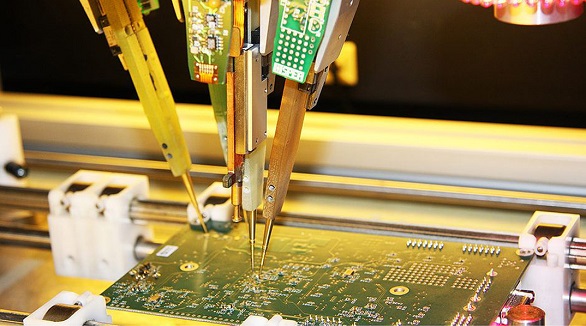
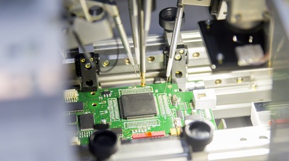
The test fixtures of a PCB are crucial for the automation of testing. These test fixtures, mainly comprising computers, control boards, enclosures, and user interfaces, are employed for the implementation of automation in testing to ensure swiftness and consistency. For customizing and refining testing, it may also include features such as metal enclosures and 3D printed components.
The quality of the PCBs will be guaranteed by choosing the right partner in manufacturing. The manufacturers must be in a position to provide competent and experienced test engineers to handle the complex designs of the PCBs and the test specifications effectively.
Conclusion
Functional testing is an integral part of the PCB manufacturing process to ensure that every board delivers on its promise with no faults and failures. This is done to make sure that the highest standards of reliability and quality are met in order to gain the trust of the customer. The functional test will be elaborated upon in the following so that this step may be understood for what it is, and how important it is for stakeholders to make informed decisions regarding their PCB assembly.
Hot Tags:
Contact us

If you can't find what you're looking for, please contact us.
Article

With SMT assembly at the forefront of electronics manufacturing, advanced inspection technologies like visual, AOI, ICT, and X-ray are essential due to increasing component complexity. Inspections throughout all stages—incoming, process, and post-reflow—address defects, ensuring quality and reducing rework.

Flying Probe Testing ensures high-performance, durable PCBs and PCBAs by detecting issues like shorts and capacitance mismatches, speeding up production, and reducing costs.

Flying Probe Testing (FPT) is ideal for low-volume PCB assemblies. It uses mobile probes and advanced features like PDM and HVS for precise, cost-effective detection of shorts and opens.
