- Products & Capabilities

- Simulation Design & EDA

- About
- Resources
Ground Loop PCB Techniques


Ground loop control in PCBs is essential to prevent EMI and signal degradation, using ground planes, star grounding, and isolating signal grounds.
In the intricate world of electronic design, ground loop control is a complicated problem, at the heart of ensuring the reliability and performance of printed circuit boards (PCBs). If you've ever wrestled with the constant hum of an audio system, then you've felt one of the common symptoms of ground loops. This article explores the complexity of ground loops and writes about a range of techniques to eliminate them, thereby enabling equipment to function more accurately and with greater reliability.
Fundamentally, a ground loop results when two or more pathways of connection have a common point of grounding in a circuit, causing electrical loops to be formed. This can cause unwanted situations where the currents take unintended paths and create potential differences among various points of the system. The sound of hum in audio systems is just the tip of the iceberg in ground loop effects.
Significant issues induced by ground loops are:
Electromagnetic Interference (EMI): Ground loops can act as antennas, inadvertently receiving or radiating unwanted electromagnetic signals. The interference can significantly decrease signal integrity, resulting in erroneous data on communication lines or deformed signals in sensitive equipment.
Signal Degradation: Ground loops introduce noise in analog and digital circuits. The noise, unwanted, finds its way onto the signal path, degrading audio, video, or data streams severely.
Damage to Components: Ground loop-generated voltages and currents of flow can lead to not just operational errors but even permanent physical destruction of sensitive electronic components.
Ground Loop Mitigation Necessity
In addition to the direct interferences, ground loops create more profound electronic design problems. Ground loop cancellation is not merely a noise cancellation issue; it's one of the issues of operational integrity and safety in general. Properly grounded circuits protect the system from charge accumulation that otherwise would present actual electrical shock risks or system failure.
For any electronic circuit to work at its best, a loop of current must be closed, usually facilitated by a proper grounding method. Ideally, ground points must be of zero resistance and capacitance, with equal potential throughout the circuit. However, the physical constraints of actual components, such as wire resistance and parasitic capacitance, result in ground potential variations that allow the unwanted currents that characterize ground loops.
Effective Ground Loop Elimination Methods
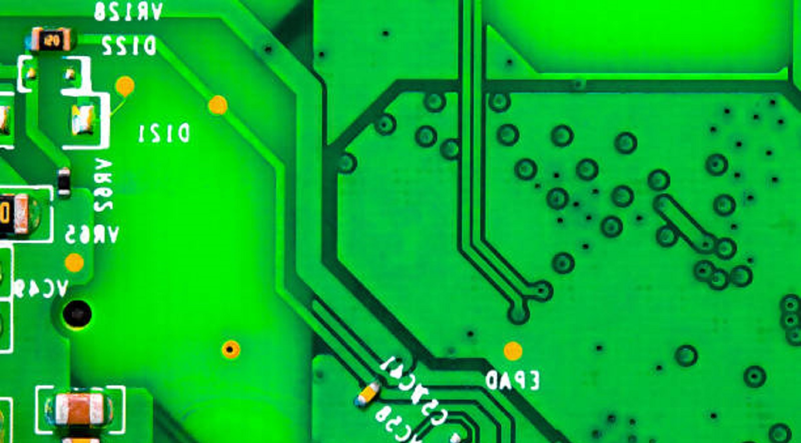
Use of Ground Plane
An uninterrupted ground plane is one of the most effective countermeasures to ground loops. It provides a low-impedance path for return currents, thus reducing potential differences between the PCB.
Two-layer PCBs: In two-layer, it's preferable to allocate one layer to the ground plane and reserve the other side for signal tracks. Limiting signal tracks on the ground plane maintains its functionality.
Four-layer PCBs: In these designs, the designers should reserve an entire layer for ground. Not only is this layout less prone to inductive coupling of currents but it also establishes a solid ground potential, thereby rendering the existence of ground loops nearly impossible.
Other than inhibiting loops, ground planes also make efficient heat sinks, suppress potential crosstalk, and enhance the general stability and performance of the circuit.
Star Grounding Technique
Star grounding combines all the grounds together and runs them back to a single common point, separating them from common impedance and blocking differences in potential among devices.
It is well-suited to work on small PCBs but may also be well employed strategically at significant nodes on large systems to achieve the same ground potential.
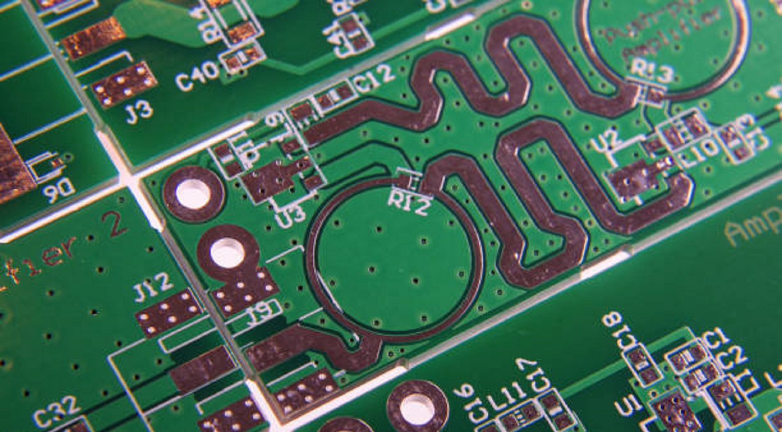
Connection of Layers via Vias
Vias are instrumental in maintaining ground continuity through several layers of a PCB, particularly in multi-layer constructions. Vias preclude the chance for inadvertent circular routes of current flow, therefore avoiding the creation of ground loops.
Optimization of Ground Connectors
To prevent impedance mismatches that may cause oscillations and follow-up ground loop formation, PCB designs are facilitated by the provision of extra ground pins. Allowing about 30-40% of the connector pins to be used for grounding, the designers can provide stable paths for current flow while avoiding loop creation.
Analog and Digital Ground Isolation
Mixed-signal environments are especially problematic, as digital signals by their nature produce high levels of noise that will interfere with the more delicate analog signals. Isolating such grounds prevents cross-talk and interference, leaving both forms of signals intact. There are situations in which it will be necessary to connect them at one strategic location, but isolation typically offers the best solution for clean and precise signals.
Applying Decoupling Capacitors
Decoupling capacitors, strategically located close to the integrated circuits (ICs), play a crucial role in stabilization of power delivery as well as reduction in noise levels. These components avoid EMI, constituting a part of any approach for prevention of the ground loop effects. Utilizing the capacitors with high and uniform capacitance between all ICs offers optimal protection against interference.
Ground loop control is a critical process in designing dependable, high-performance electronic circuits. By using such techniques as continuous ground planes, star grounding, and signal grounds isolated, you effectively eliminate the destructive influence of ground loops.
It is necessary to remain updated about new grounding practices as technology improves. PCBX is a forerunner in providing cutting-edge PCB solutions and offers professional service to assist you in attaining and exceeding all design specifications.
Hot Tags:

Contact us

If you can't find what you're looking for, please contact us.
Article
Heat sinks are essential for reliable PCB design, managing heat in high-density components like transistors and LEDs, ensuring optimal performance.
 2025/02/06
Preheating PCBs enhances soldering by reducing thermal shock, improving wetting, and activating flux, using methods like conduction, convection, and IR.
2025/01/24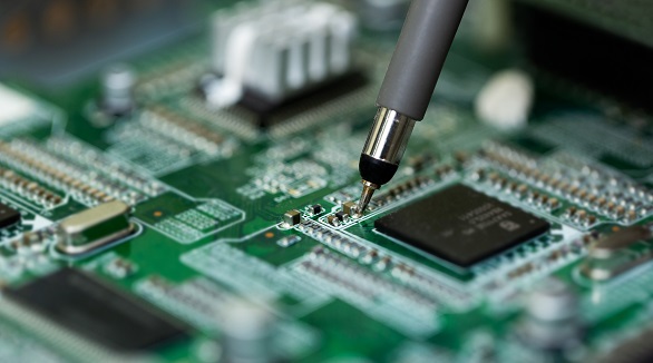
PCB short circuits arise from unintended connections, leading to safety risks. Prevention involves isolation, inspections, and thermal protection, ensuring device reliability and safety.
2024/10/23