Ground and Power Planes' Significance in PCB Design
Power and ground planes in PCBs ensure signal integrity, manage heat, and minimize EMI, crucial for efficient, high-performance electronic devices.
Power and ground planes are the crucial basic entities in the dense circuitry of printed circuit boards for a variety of electronic devices to function. They do way more than just powering and grounding; they also play an important role in ensuring signal integrity, reduced electromagnetic interference, and thermal management. Knowledge of how these planes should be successfully implemented will help in creating efficient and reliable PCBs in applications that are both complex and high-performance-oriented.
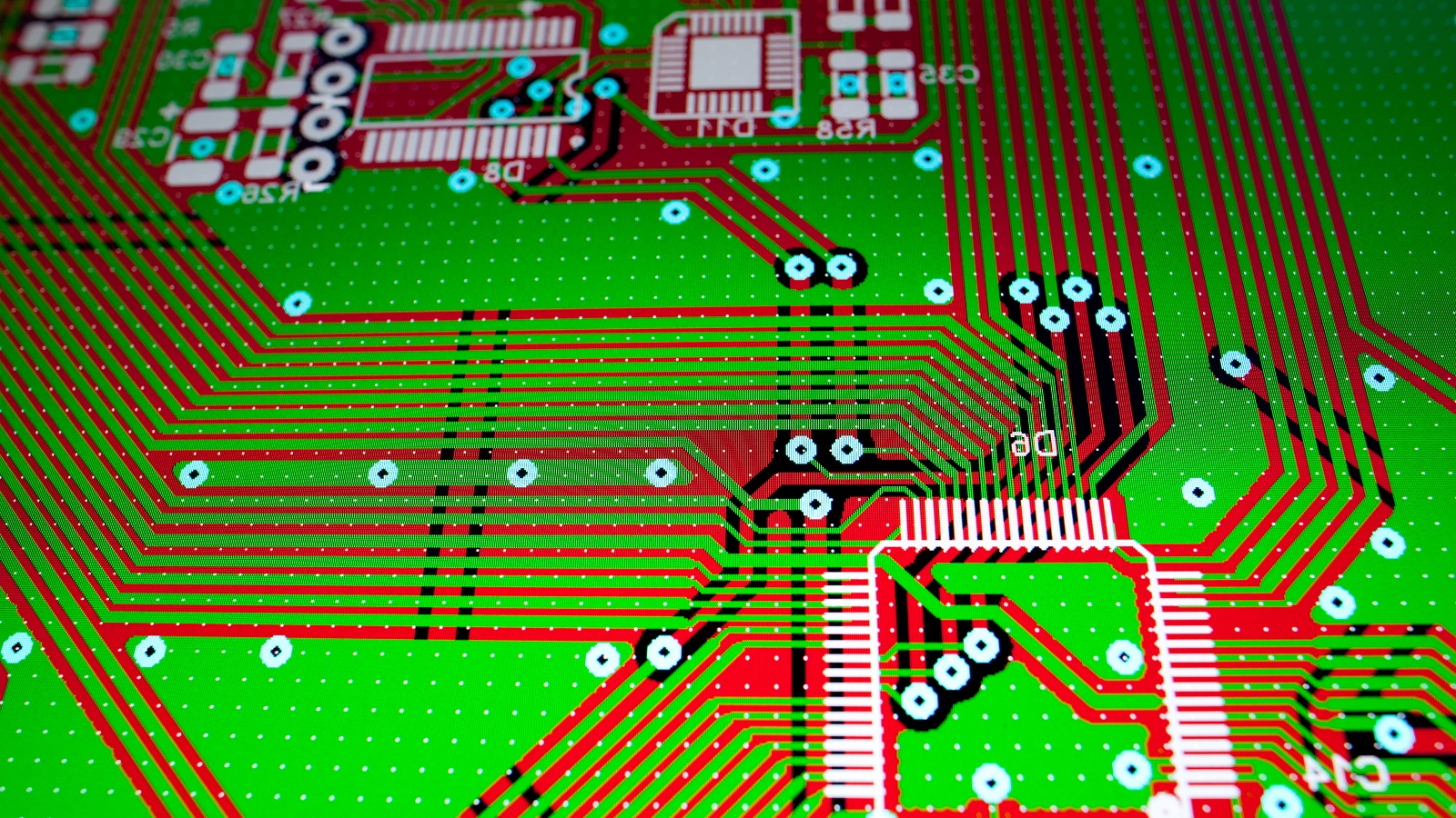
Power and ground planes are great uninterruptive sheets of conductive material inlaid in a PCB. The power plane, sometimes called the power layer, provides equally distributed power supply voltages to all parts on the board. The ground plane provides a common reference and return path for electrical signals so that stability within the circuit is maintained. These planes, which also include the ground plane antenna design, form a critical component in defining the performance of a PCB.
Advantages of Power and Ground Planes
Enhanced Signal Integrity: The ground plane ensures a low impedance return path for signals; as such, it minimizes voltage drops and noise. Power planes maintain stable power feeding, crucial in avoiding brown-out conditions during sudden surges in power demand.
Thermal Considerations: Both power and ground planes distribute the heat evenly across the PCB, hence giving good thermal performance of the board without resorting to expensive additional cooling mechanisms. This becomes more critical in boards with high power density.
Reduced EMI: Ground planes also act like shields that help to reduce the EMI emitted by the PCB and inhibit external noise from penetrating to the PCB, thereby enhancing signal fidelity and helping comply with EMC standards.
Simplified Routing and Higher-Density Designs: These planes simplify circuit designs by eliminating the need to manually route individual power and ground traces. This allows for higher density layouts that are vital in today's modern compact electronic systems.

Design Considerations for Power and Ground Planes
Current Return Paths: A huge amount of attention needs to be given towards return current paths so that signal degradation is avoided. In multilayer PCBs, the path of return should be as short and direct as possible. Seamless return paths can be created across vias for stitching grounds and power planes across layers.
Layer Stack-Up Optimization: It reduces the problem of signal crosstalk and impedance discontinuities through the optimization of layer stack-up. For instance, placing signal layers next to ground planes can be used for low inductance paths.
Separation in Mixed-Signal Designs: In mixed-signal PCBs, sensitive isolation of analog and digital ground planes may be necessary to avoid interference. This is the area of the application of ground plane antennas with isolated or linked grounds, which in turn are designed with a purpose either with net ties for maintaining signal integrity or with capacitors.
Decoupling Capacitors: Placing decoupling capacitors between power and ground planes can have the effect of creating lowimpedance paths for transient currents, reducing EMI problems and preventing voltage fluctuations.
Problems and Solutions
Challenge: Cross-talk and Signal Degradation:
Solution: Include enough spacing. Make sure to use vias to keep the distance between separate signals and planes, especially when the design is on a mixed-signal format.
Challenge: Power Integrity and Voltage Drops:
Solution: Use thicker copper layers with rightly-sized power layer stack-ups to make sure the power across the PCB is distributed evenly.
Ground Plane and Power Layer in High-Frequency Application
In RF applications, especially those of high frequency, the work of the ground planes extends to acting like a ground plane antenna to optimize the RF performance and assist signal propagation. Power layer modulation should be carefully done to retain signal integrity without allowing noise into sensitive circuits.

Power and ground planes are equally important in the PCB design. This will ensure that signal integrity, thermal management remain robust, and EMI is at a minimum. At PCBX, the importance of these planes is first and foremost when we speak of developing cutting-edge PCBs. A proper approach to the integration of power planes along with the ground plane antennas allows a designer to improve considerably the reliability and performance of their electronic systems.
These are increasingly complex times with regard to the use of electronic devices, and the strategic use of power and ground planes in the design of efficient, high-performance PCBs plays a fundamental role. Such elements are used to provide a means for designers to push technology boundaries and ensure stable and reliable products for today's dynamic and demanding marketplace.
Hot Tags:
Contact us

If you can't find what you're looking for, please contact us.
Article

PCB panelization consolidates multiple PCBs into a larger board, improving manufacturing efficiency and reducing waste. Techniques include V-scoring and tab-routing. Proper design enhances assembly, testing, and cost-effectiveness.

Designing a PCB involves ten detailed steps: schematic capture, creating a blank PCB layout, syncing designs, defining stackup, setting design rules, placing components, adding drill holes, routing traces, labeling, and generating output files. These steps ensure an organized, error-free process from concept to manufacturing.

The article explains the current situation of Printed Circuit Boards and future development based on efficient production helped by advanced software and manufacturing processes. Future technological developments are in store for 3D Printed Electronics, flexible PCBs, eco-friendly biodegradable PCBs, and board cameras. It elaborates on other powerful automation tools that are going to make the entire PCB design process efficient in the near future. All of them will further improve and develop with the technological advances in PCBs, keeping up with the ever-increasing industry and consumer demands.
