Guidelines for DFM in PCB Design
DFM ensures cost-effective PCB design by optimizing size, layers, materials, and components, focusing on manufacturability, reliability, and process efficiency.
Design for manufacturability, or DFM, is an important design consideration in a functional, reliable, and testable design that will be efficiently and cost-effectively manufactured. Understanding the basic steps of manufacturing, key cost drivers, and best practices throughout the design process can help an engineer optimize their designs for manufacturability.
Common Cost Drivers in PCB Projects
Several factors can affect the price of a PCB project. First, it will be the size of the board itself, but other influences are how many layers it is, what nonstandard parts are included, whether the board requires special materials, and via sizes for manufacturing and assembly.
Material selection will have great variations in cost. Applications such as high voltage or high-frequency designs may require special materials, but projects with different requirements will not take full advantage of costly materials without functional benefits. Substrate material selection would involve parameters concerning thermal performance, electrical characteristics, and layer count. It is also possible to increase the costs by changing the thickness of copper and finishing, which may be required depending on specifics for the targeted application.
Component Selection and Layout Influence on Manufacturability
Hybrid designs have both SMT and THT components, which result in more cost due to different assembly processes. It is better to avoid those hybrids rather than use only SMT design. If the designer is bound to use THT components, then it is better to segregate them from SMT parts on opposite board sides. In a case where THT is on the top and SMT is on both sides, manufacturers charge more because of epoxy consumption during assembly.
Annotation is important: parts should be annotated with applicable silkscreen designators, such as type, unique numbers, polarity designators and special pin designators. Good clear annotations make verification and troubleshooting easier to perform after production. Text should be oriented to match component orientation and should not conflict/overlap each other, or IC pin designators will not be readable with chips installed.
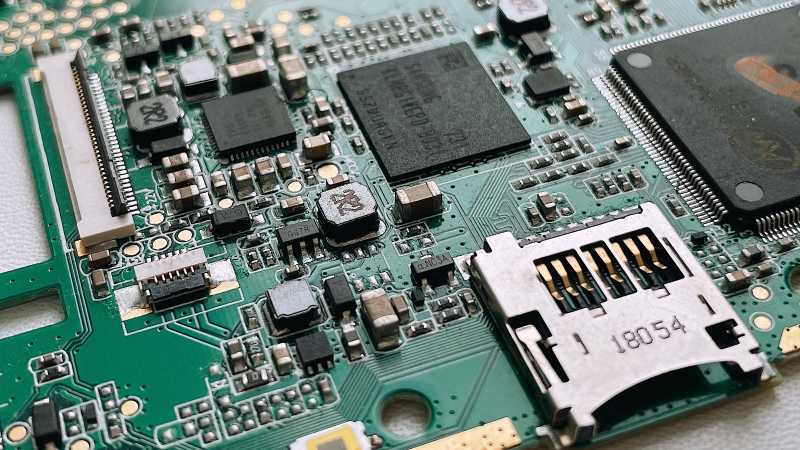
Via Best Practices for DFM
The width of a via should not be closer to any conductor or to a plane edge than the width of that conductor, or there are specific design conditions allowing such placement. Plated vias shall be in a minimum 1:1 aspect ratio with the substrate thickness of the board, as this will ensure adequate copper build-up during fabrication. The annular ring width shall be ample enough to avoid becoming subject to lifting during soldering, and capable of supporting structural integrity during operation, especially when the drill hole may be somewhat eccentric.
Clearance between exposed vias not connected to stitched pads and other conductors should be around 0.15"-0.2". Tented or plugged vias are preferred for most design especially on BGA designs where vias are located near the component's solder pads. For other ICs, do not place vias under the chip unless necessary to implement thermal relief to avoid solder wicking that may cause short circuits.
Trace Routing Guidelines and Test Points
Teardrop pads can avoid production issues occurring at thin trace to larger pad and via junctions. Trace necking allows soldering with enough solder joint that might be formed during soldering for long traces or those traces joined with large pads. Fan-outs of traces should be done between two nearest components or nearest pins in order to avoid tombstoning and cold solder joints while soldering.
Critical nodes and locations placing test points on the PCB, where they do not crowd, enhance testing and troubleshooting.
Component Placement and Solderability Considerations
When designing for manufacturability, especially with wave soldering processes, orient components for optimal soldering. Larger components should not shadow smaller ones; pins are oriented such that they solder simultaneously as they pass through the molten solder. Consistent orientation of similar components enables efficient assembly. Distribution of devices evenly across the board can be helpful, too, when trying to maintain thermal balance to prevent warping during assembly.
Influence of PCB Classes on DFM
Classes of PCBs define quality and reliability for a particular application, from class 1 all the way up to class 3, with critical applications such as aerospace and medical devices. Class 1 boards are all about cost reduction, whereas class 3 boards have to be extremely stringent with their DFM measures, so their quality and reliability can be of the highest standard.
For class 1, there is normally no special DFM requirement, while class 2 requires a master drawing with physical dimensions in it besides coating thickness and board plating. Materials, processing conditions, and design concepts are duly documented under class 3 in order that the most exacting standards may be satisfied.

DFM is equally an essential discipline in PCB design, focused on functionality, reliability, and effective cost through the manufacturing process. Understanding manufacturing processes, understanding cost drivers, and incorporating best practices during design helps designers optimize for manufacturability. Appropriately sizing, layer count, material selection, component placement, and accounting for PCB class and coupons go a long way in making production successful and efficient. These rules, stressed from the very beginning, will make sure that your PCB designs meet the demands of current technologies and high-performance requirements.
Hot Tags:
Contact us

If you can't find what you're looking for, please contact us.
Article
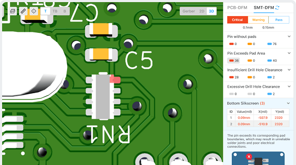
The article is developed concerning the breakthrough of integrated circuits and the need for custom PCBs in some electronic products. It enumerates ten golden rules in conducting PCB layout design and manufacturing: grid selection, routing, power layers, component placement, panel duplication, component value combination, frequent DRC, flexible silkscreen use, decoupling capacitors, and pre-production parameter checks. These rules provide for the optimum design and manufacturing of a PCB.
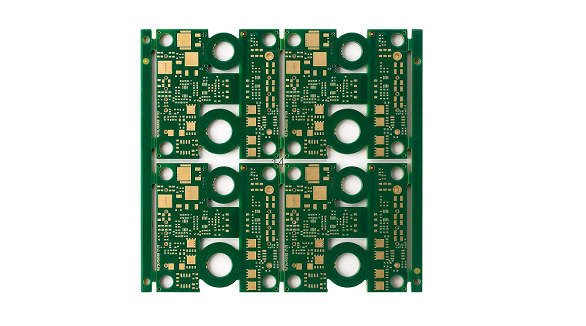
Most electronic circuits are mounted on PCBs, or Printed Circuit Boards, which provide mechanical support and electrical interconnection of electronic components. There are, however, special applications that involve the use of single and double-sided PCBs, multi-layer PCBs, or even rigid and flexible PCBs with aluminum backing, targeting medical, industrial, auto, and aerospace industries. They may use materials such as fiberglass, epoxy, aluminum, and others.
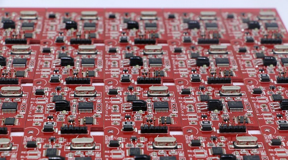
Thermal management is all about more than just keeping the temperature of electronic systems and printed circuit boards low. It has been a key issue related to reliability and performance. Of the very basic fundamentals that would be studied in the field, some are concerned with methods of heat transfer. These are through conduction, convection, and radiation. The methods of cooling include natural cooling, forced-air cooling, fluid cooling, and evaporation cooling. Appropriate thermal design rules shall be followed wherein the chosen materials provide optimum thermal conductivity and the components of a system are so laid out that no hot-spotting will take place. Thermal analysis becomes critical in pointing out heat-related issues and optimizing the design. It thus minimizes failure rates and enhances stability and functionality of the electronic systems through comprehensive thermal management.