- Products & Capabilities

- About
- Resources
How to Avoid Common Wave Soldering Issues


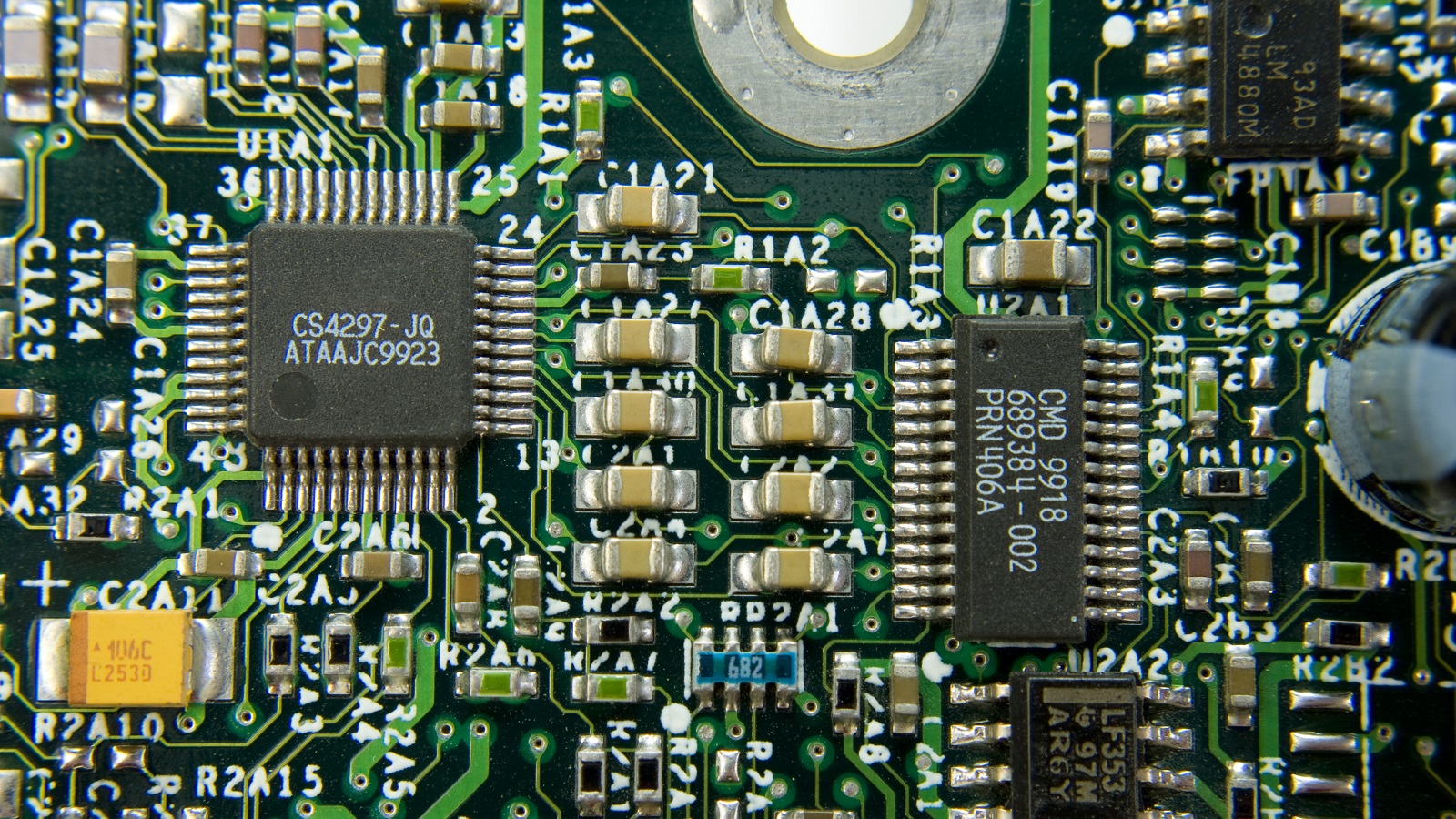
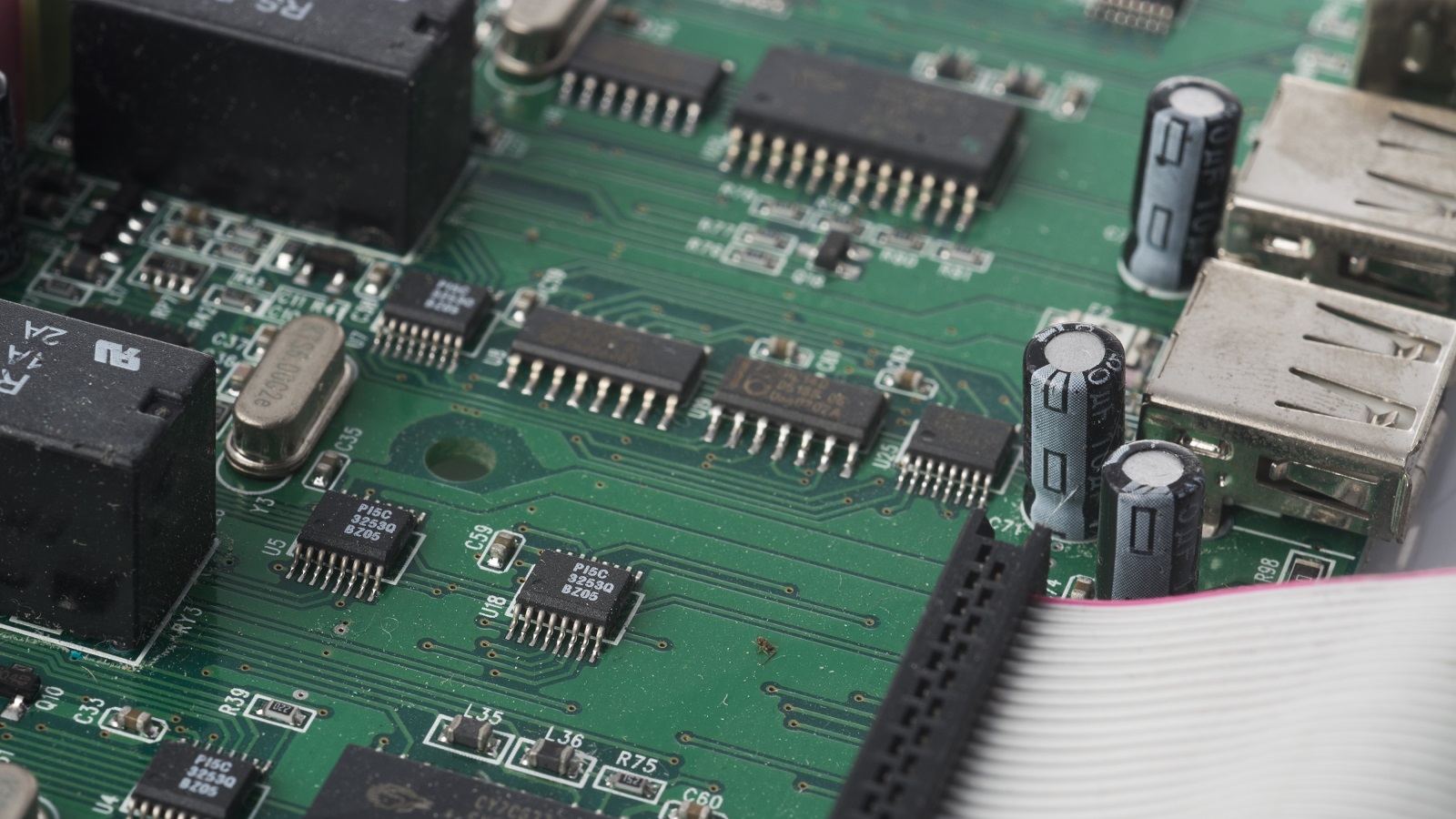
Wave soldering is vital for assembling printed circuit boards (PCBs), aiming to bond electrical components. The process involves passing PCBs over a wave of molten solder to form connections. Common defects include pin/blow holes, solder shorts, poor hole fill, lifted components, excessive solder, solder balling, and solder flags. To address these issues, key factors include proper flux application, controlled preheat temperatures, optimal solder wave settings, and careful material handling. Understanding and managing these factors ensures high-quality, reliable PCB assemblies.
Wave soldering is one of the most important processes in the assembly of a printed circuit board that aims to bond electrical components such as resistors, capacitors, and LED lights into the board. In essence, the process involves mounting the respective components onto a PCB, which is then passed over a wave of molten solder that flows like glue. The molten solder wets the exposed metallic areas, forming a reliable mechanical and electrical connection. Though very effective, this process is subject to some defects that will be reduced by proper knowledge and control. This article expounds on some common problems in wave soldering and how to resolve them.
Pin and Blow Holes
Pin and blow holes are defects characterized by small, usually round voids or holes in the solder joint caused by gas trapped within the PCB during soldering. These holes can form either by a single burst of gas or by continual gas break-through. The difference between pin and blow holes is normally based on the size of the defect, though they really do describe the same problem.
The quality of the PCB itself again is key to addressing pin and blow holes. Assuring a minimum of 25 µm of copper plating inside the through-holes will dramatically reduce this issue. In addition, baking the boards before soldering will help to dry out excess moisture from the boards and thus defects related to moisture can be avoided. This, however, cannot totally eradicate the root causes, such as gas being trapped due to inferior plating quality. This shows the requirement for better materials and processes in making these Printed Circuit Boards.
Solder Shorts on PCBs
Solder shorts are becoming more common due to the fact that component pitch, the space between terminals, is getting smaller. Historically, pitches were of the order of 0.050 inches but have now shrunk to as small as 0.02 inches, greatly increasing the potential for solder bridging between leads.
Solder shorts occur when the solder doesn't properly break off between two or more leads prior to hardening. This can occur on the top side of the board, often because too much pressure was applied while applying solder. Shrinking the size and length of the pads will decrease the volume of solder the board can hold, thereby reducing the occurrence of shorts. The solder wave height and conveyor speed can also be adjusted properly to control the quantity of solder dispensed to prevent excessive solder bridging.
Poor or Non-Uniform Hole Fill
Poor or non-uniform hole fill is another common defect wherein the solder wets the leads but cannot fill up the through-hole properly. This may be due to insufficient application of flux, low temperature while preheating, or a change from foam fluxing to spray fluxing since it usually reflects upon the poor penetration of the flux into the holes.
In all cases, the preheat temperature of the PCB should be kept between 100-110°C to ensure uniform hole fill, particularly for multilayer and double-sided PCBs. For single-sided PCBs, less preheat temperature is usually needed since the solder doesn't have to flow through multiple layers. A fine application of flux with complete penetration, coupled with getting a constant temperature profile in wave soldering, is the recipe for uniform hole fill.
Lifted Components
Tombstones, also called lifted components, occur due to physical and thermal issues during wave soldering. Heat obtained while soldering may weaken the adhesion of copper on a PCB and cause component lift-off, especially when force is applied to the board.
Therefore, handling the board gently when it is being soldered and also after the soldering process is highly essential to avoid this problem. High-thermal-resistance epoxy will enhance the overall strength of the PCB withstanding heat exposure over longer periods. Using correctly sized lead parts that do not protrude too much through the board will also help in preventing tombstoning. Thermal tolerances of the board and the components should agree with each other to ensure there are no disparities in solderability, and the components will not lift off.
Poor Hole Fill
Another hapless defect common to wave soldering is inadequate hole fill. This occurs when the amount of solder that fills the pre-drilled holes in a PCB is not sufficient, thus leading to poor electrical connections.
There are many factors to consider with respect to poor fill. Inadequate flux application—which may not have penetrated the board—can prevent solder from rising through the holes due to lack of activation. It's extremely important that the top side of the board reaches the correct temperature—typically in the range of 150 to 170 degrees Celsius—because solder always flows toward heat. If the temperature is too low, the solder won't flow properly.
Taking a temperature profile of the wave solder process can help ensure that correct heat settings are maintained throughout. This should closely match the reflow processes for the board to ensure uniform heating. Finally, adjusting the board height could promote full exposure to the solder wave, which would then allow for the hydrostatic pressure needed to fill the through-holes. Ensuring adequate volume and proper application of flux also help in reducing insufficient hole fill by enhancing solder wetting capabilities.
Excessive Solder
Excessive solder buildup may present practical problems even when there is still electrical connectivity between the board and the component. The excess solder can mask component pads and leads, thereby obstructing any attempts to inspect and check the connections.
This condition can be avoided by having similar components oriented consistently during wave soldering. All like components should be oriented the same direction to allow for consistent solder application. Incorrect lead lengths can result in excess solder also. Standard lead lengths that project a proper distance through the PCB pads will prevent a swimming pool of solder. Also, conveyor belt speeds can be adjusted to help control the solder quantity applied. In case of a too-slow conveyor, several waves coat the components with solder. This can result in excess buildup. This can be best taken care of by simply coordinating with team members to agree on an acceptable speed for the conveyor belt.
Solder Balling
Solder balling is a common fault whereby small balls of solder, after wave soldering, stick to the PCB near the lead ends. Such a defect may arise due to very high temperatures in the solder, the formation of splashback from the solder wave, or gases issuing out from heated flux.
Two of the more important ways of reducing solder balling include good PCB design and proper selection of a solder mask. Also, using a solder mask with low adhesion to solder can enhance the durability of the board and improve its performance. Checking the height of the wave itself and adjusting all parameters can prevent solder from splashing back. If issues with solder balling are related to flux gases, ensuring adequate levels of air and nitrogen levels in the environment around the solder tank can reduce flux-related problems. Run tests with a white card over the solder wave with and without boards to understand the root cause of solder balling and correct it.
Solder Flags
Solder flags are small protrusions of solder from component leads that indicate improper flux application and solder drainage problems. If solder drains too slowly from the wave soldering machine, excess solder may remain on the leads and result in flags.
Proper control between the solder wave and the board is essential in separation. The backflow can be set up for a "lambda"-style wave to provide a constant direction and speed of solder flow, which helps to reduce the formation of solder flags. Proper flux application is important for adequate wetting of the leads and proper solder drainage. The leads themselves can be oxidized as a cause of this problem. Finally, solder flag formation can be reduced by ensuring correct storage to prevent the oxidation of leads in-house, or verifying suppliers' practices on cutting and storage.
Conclusion
Wave soldering is the most effective method for assembling electrical components on a PCB. However, a number of defects, such as pinholes, solder shorts, inconsistent hole fill, lifted components, and solder buildup, can easily occur. Understanding these defects and proper preventive measures is key to attaining high quality in soldered connections and reliable PCB assemblies.
Much of these common wave-soldering problems can be overcome by correct application of flux, proper temperature, solder wave parameters correctly set, and proper material handling. Hence, proper process management and an understanding of the intricacies of wave soldering will ensure success in any mission relating to PCB manufacturing: quality, dependable electronic products.
Hot Tags:

Contact us

If you can't find what you're looking for, please contact us.
Article
Wave soldering quality hinges on several factors: consistent solder contact, precise heat management, optimal separation speed, and controlling solder surface tension. Key considerations include deoxidizing surfaces for effective wetting, strategic lead/pad design, and correct component orientation. Mastering these variables enhances PCB assembly reliability.
 2024/08/23
Soldering forms a very important part in the assembly of a PCB. Wave soldering is ideally applied in Through-Hole Technology, while reflow soldering in Surface Mount Technology. Wave soldering involves flux spraying, pre-heating, soldering, and cooling, while in the case of reflow soldering, pre-heating, thermal soak, soldering, and cooling steps are applied. Temperature and time control are the two most critical parameters in the above-mentioned techniques for ensuring soldering reliability.
2024/07/26
Ball Grid Array (BGA) components, such as PBGA, CBGA, CCGA, TBGA, and CSP, provide high I/O density, improved reliability, and high-quality electrical and thermal performance. Quality assembly and functionality are assured since advanced soldering and inspection methods are required, like AXI and AOI. Proper storage and handling shall guarantee the performance of the devices.
2024/07/26