How to Balance Integrity and Manufacturability in PCB Design
PCB design demands precision, using subcircuits for optimized layout, managing thermal concerns, and minimizing signal paths to ensure performance and manufacturability.
In the grand dance of modern electronics, printed circuit boards serve as the critical foundations that maintain component connectivity. The path from a schematic diagram to a functional PCB layout is rather precise and detailed. The process requires not only attention to reducing the dimensions of the board but also achieving important objectives such as signal integrity and manufacturability. It's not about connecting the dots; it means creating a robust blueprint to sustain reliability in operation and scalability in production. In this article, we look at some advanced approaches to PCB design, signal integrity, and manufacturing efficiency balance.
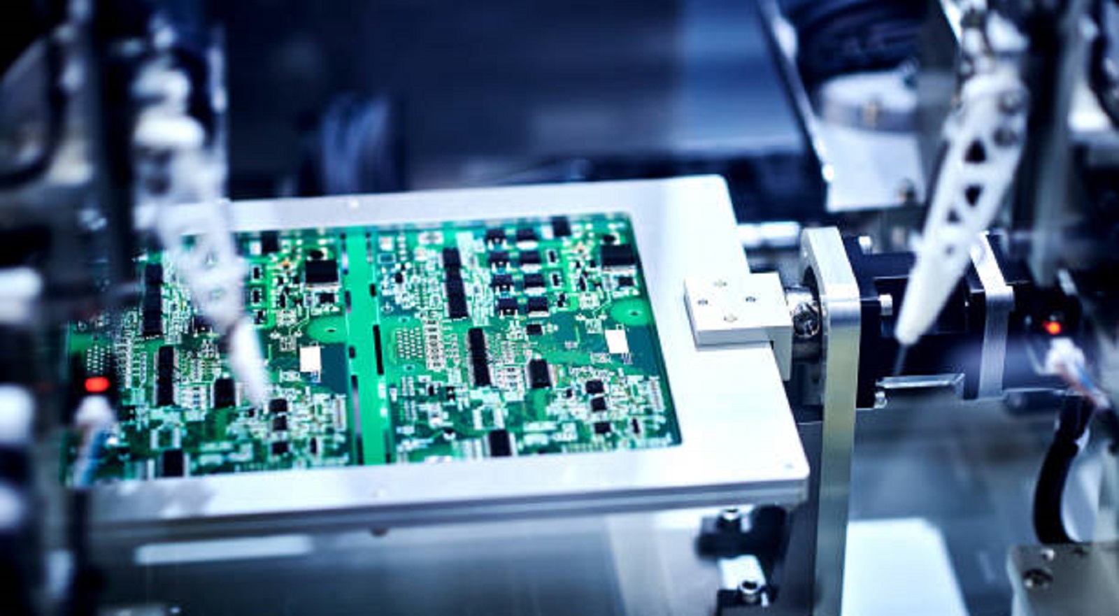
Subcircuits: Guiding Precision in Component Placement
Being able to identify subcircuits in a PCB design is a strong approach that directly dictates component placement and routing efficiency. By isolating specific functional blocks, a designer can strategically place components to ensure that space is efficiently utilized while signal pathways are as short as possible. This will minimize cross-talk and reduce the decay of signals so that the sensitive low-voltage areas do not get the interference from the high-voltage sections. Accurate identification of subcircuits not only helps in the integrity of signals but also supports the board in its safe and reliable operation.
Another important consideration would be to leave room for decoupling capacitors and vias, especially when there are digital ICs on the design. Decoupling capacitors try to dampen these power supply fluctuations by filtering out such sudden changes in power demand. Adding more vias can further raise capacitance, ensuring a dependable supply when transient demand suddenly peaks. This foresight not only strengthens signal integrity but also avoids issues such as brownouts that may affect circuit performance.
Thermal management also plays an equally important role in deciding the placement of components within subcircuits. The heat-sensitive components must be consciously kept away from the generating parts, assuming that the even PCB acts as a heat sink. It is essential to maintain the component characteristics and to ensure uniform performance. Adequate clearance for the externally mounted heat sink and mindful placing of sensitive parts from heating prevent thermally induced failures.
Routing: Creating Paths More Than Just Connectivity
The routing in the PCBs is not exactly putting conductive material between components. Routing in itself is a deep process. From the point of making the board work to considering manufacturability and the physics or electrical properties of the conducting material, it can be considered thoughtful work for space optimization.
This minimization of trace length is one of the bases of good routing. The longer a trace is, the larger its resistance becomes and thus the higher its signal attenuation is. Lengthy traces, on the other hand, also pose a threat to signal decay because they might work like antennas, receiving or sending EMI. Keeping traces short is preferred even in cases of non-critical designs where strict impedance matching may not be of any concern.
Trace width also plays a significant role in circuit impedance and noise susceptibility. While narrower traces provide better noise immunity, they should still support current demands, especially when carrying power. In high-frequency applications, traces should taper into the component pads to help preserve signal integrity and reduce signal reflection. Traces that run parallel should not be placed for extended runs; instead, sufficient separation-ideally three times the thickness of the dielectric-should be maintained to reduce crosstalk.
Vias are the essential part of PCB routing that ensures vertical connections between layers. Having vias in pairs and placing ground vias close to signal or power vias enhances via inductance and hence the current return paths. These reduce signal distortion and crosstalk. In contrast, strategic placement of vias will be helpful for the general robustness and performance of the design.
Optimizing Layer Stackup in Multi-Layer PCBs
In multi-layer PCBs, traces are not isolated entities; their interactions across layers can greatly affect signal integrity. Solid reference and supply planes are essential to influence capacitance and ensure signal integrity throughout the board.
Place signal and power traces over solid reference planes, which should be typically at 0V, but in some cases, other power planes can work. Do not allow gaps in reference planes, as they will greatly expose signal traces to critical EMI issues. Such gaps may result from badly placed vias, which could cause discontinuity, leaving the signal traces vulnerable. In order to prevent electromagnetic interference, especially in sensitive applications, ensure that the signals do not cross over such gaps.
The thoughtful design of layer stackups reinforces capacitance, curbs EMI vulnerabilities, and bolsters overall PCB reliability. Solid ground and supply planes, together with decoupling capacitors, provide immunity against transient power dips, therefore reinforcing the stability of the circuit during sudden spikes in current consumption.
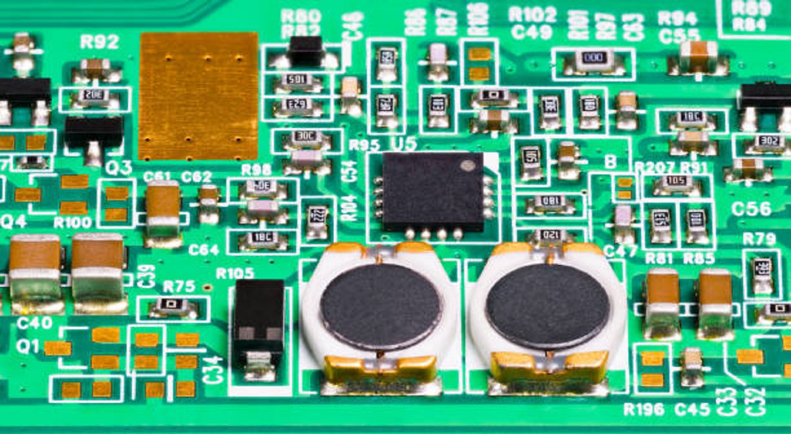
Designing a functional and manufacturable PCB layout is definitely an art, requiring acumen insight and strategic planning. Designers can ensure better signal integrity by making the most of the available space using subcircuits and keeping the pathways for signals at a minimum. Combining these with precise routing techniques can help designers overcome electrical performance and manufacturability challenges. It also includes thermal management for protecting heat-sensitive components, placing vias, and optimizes layer stackup in order to provide robustness for the reliability of the design.
As technology is continuously improving, and electronics are becoming increasingly complex, the integration of these principles into PCB design will continue to be critical in the delivery of high-performance and scalable technology solutions. The designers of PCBs who master these techniques assure functionality and enable efficient manufacturing processes, thereby guaranteeing the successful realization of innovative electronic products.
Hot Tags:
Contact us

If you can't find what you're looking for, please contact us.
Article
Castellated pads in PCB design facilitate easy board-to-board connections, enhancing miniaturization, assembly, solder quality, and flexibility for compact modules.

Capacitors are crucial in PCB design for filtering and timing. Correct polarity in electrolytic and tantalum types prevents malfunctions and ensures reliability.
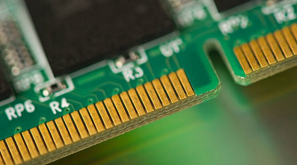
Edge connector bevelling enhances PCB durability and reliable connections, vital for frequent usage and secure engagements, with limitations primarily in plating.