- Products & Capabilities

- About
- Resources
How to Identify PCB Components


PCBs are crucial in electronics, providing a platform for component interconnection. Mastering component identification ensures effective design, troubleshooting, and maintenance, vital for device reliability and performance.
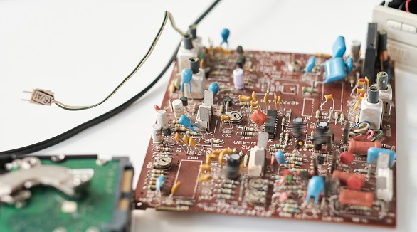
The digital era has flooded our lives with waves of electronic gadgets ranging from simple smartphones, computers, and household appliances to complex machinery in industries, all of which play their vital role. At the heart of these gadgets lies the humble printed circuit board. The PCBs form the backbone of electronics, as they offer a structured platform for mounting and then interconnecting different components. In developing this foundation, engineers and technicians must be proficient in the application of standard descriptive notation systems. Mastery of the PCB component identification art is an important factor for engineers, technicians, and hobbyists in effective troubleshooting, repair, and maintenance.
Circuit Board Basics
A printed circuit board is no ordinary compilation of wires and components but rather a very thoroughly researched piece of engineering that becomes the backbone of electronic circuits. The basic functions that it fulfills include providing mechanical support, allowing electrical connections, and assembling multiple components into one compact, orderly structure.
Types of PCBs
Single-Sided Boards: These have components mounted only on one side and are thus simpler and less expensive but with limited complexity.
Double-Sided Boards: These are boards with components on both sides that offer a higher component density and better functionality.
Multi-Layer Boards: These consist of multiple layers of copper traces sandwiched between insulating materials that allow the mounting of even more complex and denser component arrangements.
Ordinary substrates are materials such as FR-4 (Fiberglass-Reinforced epoxy) and polyimide, which provide toughness yet are insulative. Conductive copper layers are etched or deposited to form the desired circuit patterns. The solder mask and silkscreen are applied to protect traces from oxidation and for component identification.
Layers in PCBs
Copper Layers: Serve as the conductive pathways, providing electrical connections between various components.
Solder Mask: This is a protective layer over copper traces that prevents accidental short circuits and aids the soldering process by allowing only the needed areas to be exposed for making connections.
Silkscreen: Provides a visual reference for component placement and labeling. Normally, this comes in ink print, mostly contrasting with the solder mask on which they are printed.
Insulating Layers: These layers separate the copper layers from each other, insulate the layers against the occurrences of a short circuit, and provide mechanical strength.
These layered structures are meaningful, which enable one to understand such complex designs or functionality of the PCBs while helping both in designing or repairing processes.
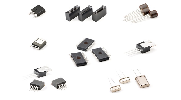
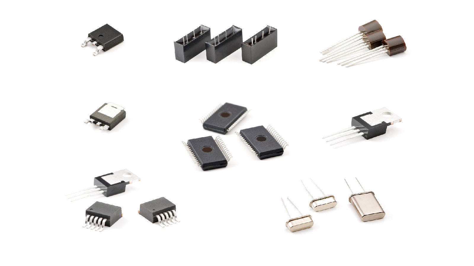
Identifying Components on PCBs
The different components on the PCB are important to understand in electronics. A breakdown into common components and their identification is shown below:
Resistors
Appearance: Cylindrical with colored bands.
Function: To limit or regulate current flow.
Identification: Color code system or numerical markings; if not sure, always check the datasheet.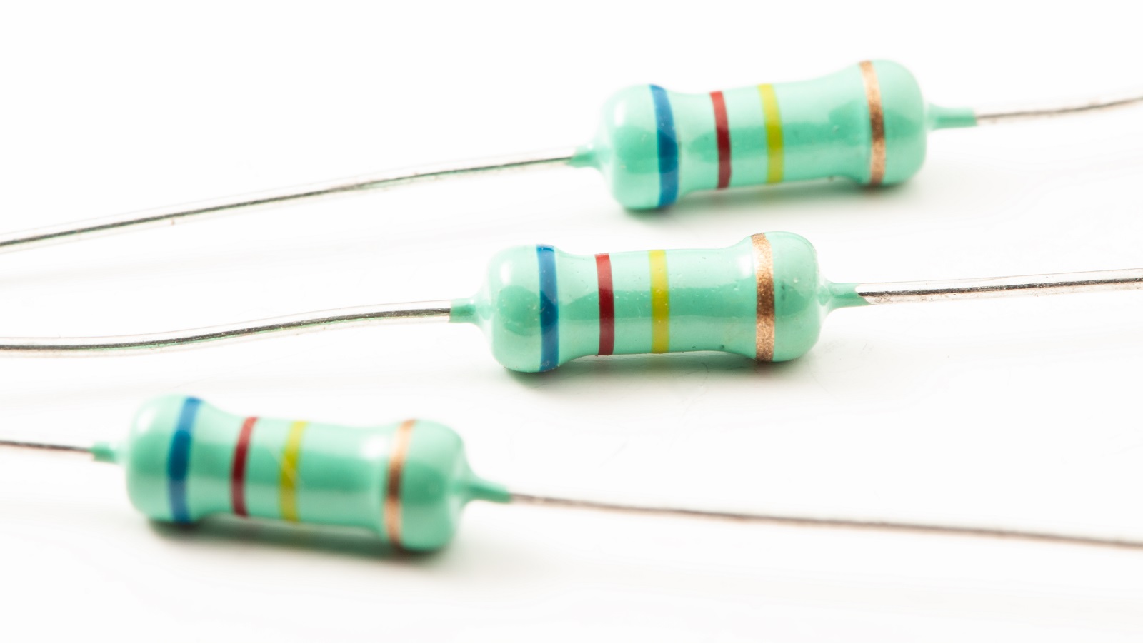
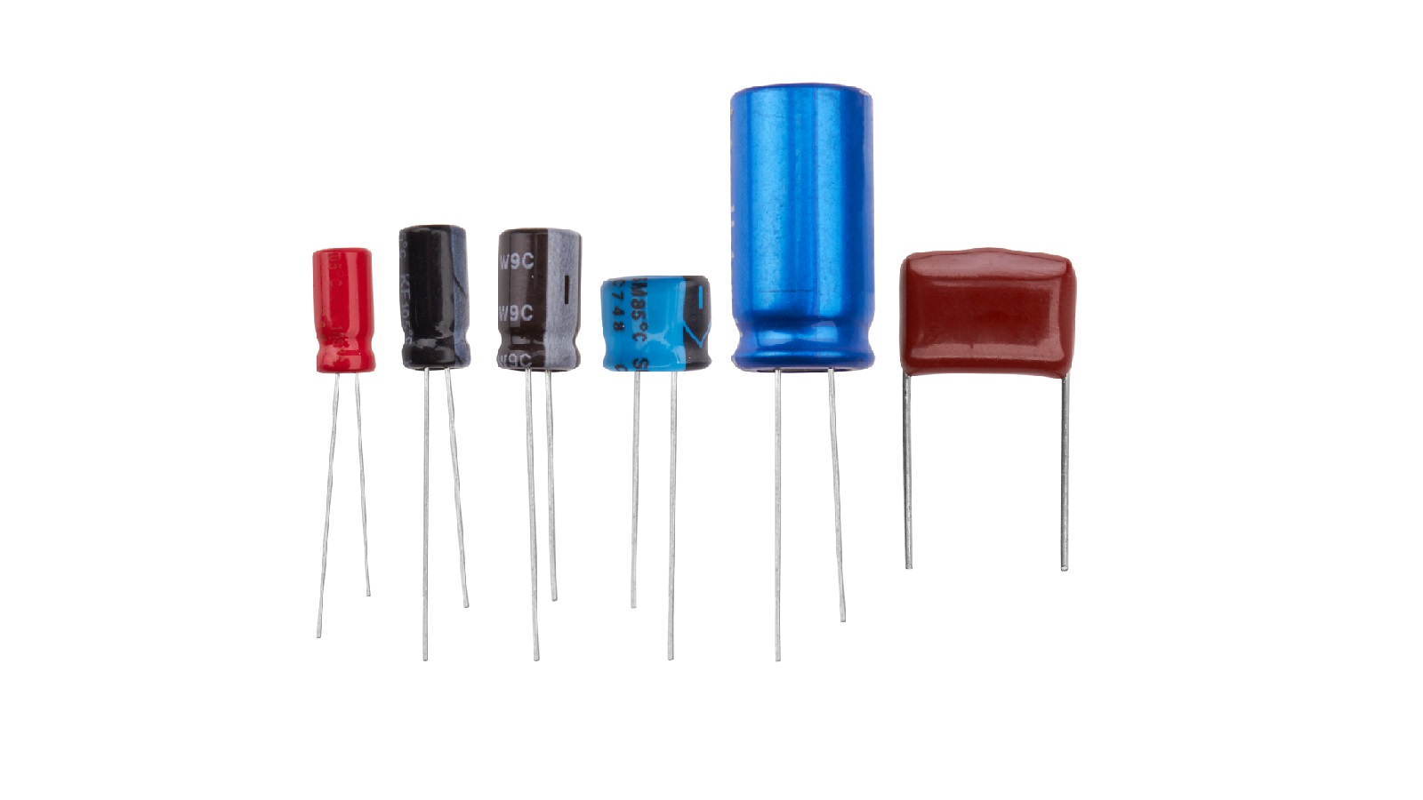
Capacitors
Appearance: Small cylindrical, box-like, or disk-like.
Function: Store and regulate electrical energy.
Identification: Capacitance value and voltage rating are usually marked on the body.
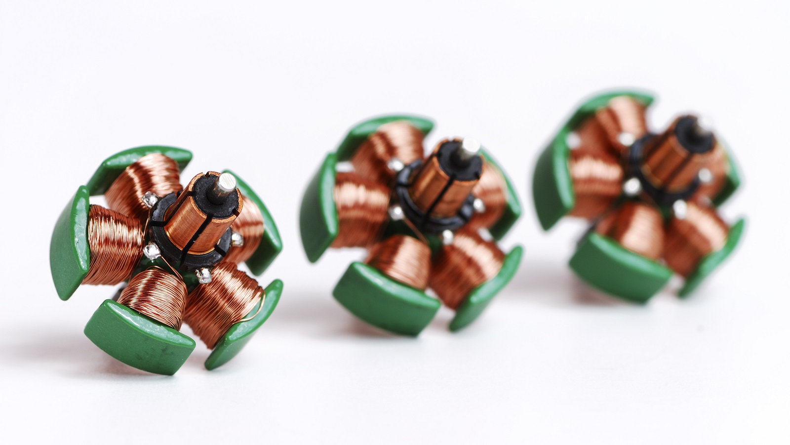
Inductors
Appearance: Coils, thus they often look like a wire with several wraps.
Function: Energy is stored in the magnetic field.
Identification: Standard code or markings can be found on the surface.
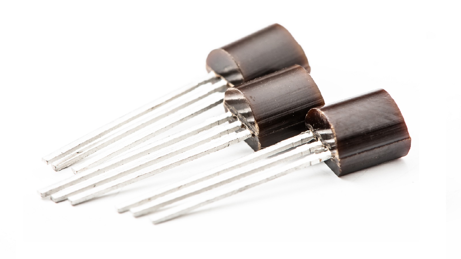
Transistors
Appearance: Small three-terminal devices; flat or rounded packages.
Function: Amplify or switch electronic signals.
Identification: Look for part numbers or refer to datasheets and package styles.
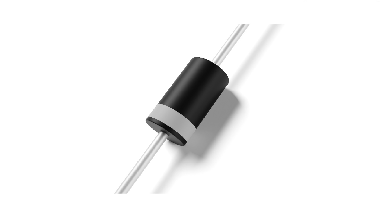
Diodes
Appearance: Small cylindrical with marks indicating anode and cathode.
Function: Allow current to flow in one direction.
Identification: Polarity markings and part number(s).
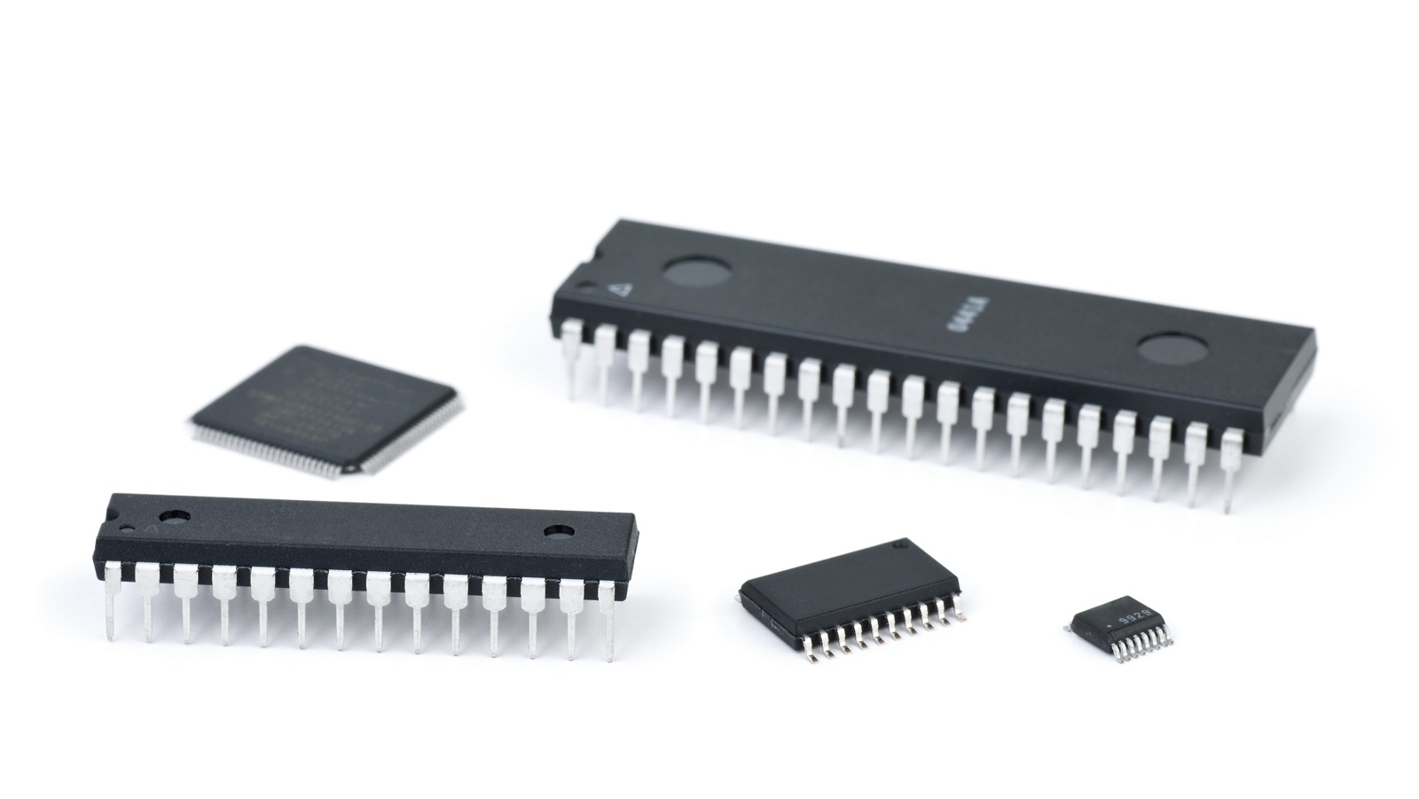
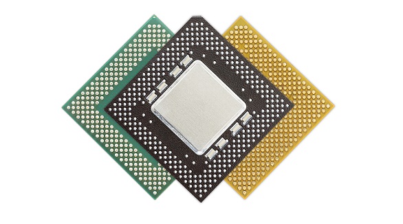
Integrated Circuits (ICs)
Appearance: Black plastic chip with a number of pins.
Function: Function is dependent on design.
Identification: Part numbers are usually printed on top of the ICs.
Switches, Relays, and Connectors:
Switches: Identified by mechanical action-toggle, push-button.
Relays: An electromechanical switch with a coil and contacts that show recognisable features.
Connectors: Allow safe electrical connections between PCBs and components.
Component Identification Techniques
Visual Inspection
First of all, identification depends on a close look at the PCB: shapes, sizes, and other visible markings should be observed. The use of magnifying tools increases visibility while strong lighting shows minute details. Use the PCB's silkscreen for component labels.
Understanding Schematics in PCBs
Schematics are the most important blueprint needed to explain how the components interconnect. They are drawn with standardised symbols, which give a graphical clue as to functionality of the circuit and help place or identify components. Being able to recognise such symbols is one of the basic skills learned in electronics.
Testing and Measurement Tools
Multimeters: These measure electrical properties such as resistance, voltage, and current. You can compare the measurements against standard values to confirm component identities.
Oscilloscopes: Very helpful in observing electrical signals, especially when tracing active components like transistors and ICs.
Specialised Testing Equipment: Some equipment, like LCR metres and curve tracers, are specifically designed to measure a particular property with high accuracy.
Advanced Techniques and Applications
Provide details of the design software used and other tools, such as CAD software, in order to develop detailed schematics and layouts. Such design tools ensure accuracy, enable simulations, and facilitate the testing process well before actual manufacturing.
Repair and Troubleshooting
Successful troubleshooting starts with a visual examination and works its way through diagnostic tools. Isolate potential faults, confirm the fault with an in-circuit tester, and use thermal imaging in searching out heat sources that can show suspect faulty components.
Documentation and Traceability
The processing and identification of components on the PCB by silkscreen printing or adhesive labels make identification easy, thus ensuring traceability. Component databases ensure that a record of parts is complete, helpful in inventory management and industry standards.
Conclusion
Understanding the components on a PCB and how to identify them is important in any form of electronic design, production, or maintenance. Good proficiency guarantees good troubleshooting, pinpoint repairs, and smoothness in procedures of maintenance. As technology is constantly evolving, greater utilization of the high-end tool shall even more improve the accuracy and speed of identification to ensure a competitive advantage in electronic design and manufacturing. Indeed, the integration of best practices in the visual inspection of components, understanding schematics, and measurement techniques allows the professional to correctly navigate the labyrinthine world of component identification on a PCB and ensure the performance of electronic systems.
Hot Tags:
Contact us

If you can't find what you're looking for, please contact us.
 2024/09/12