- Products & Capabilities

- Simulation Design & EDA

- About
- Resources
How to Manufacture a Single-Sided PCB


Single-sided PCBs, essential for simple circuits, are cost-effective and easy to manufacture. The 10-step process includes material prep, circuit design, layout printing, board cleaning, design transfer, developing, etching, photoresist removal, drilling, and optional final steps like solder mask and testing for quality.
Single-sided PCB is one of the basic necessities of the electronic manufacturing world; it is mostly used in simple circuit design. Single-sided PCB lies in the category of easy, low level, and cheap manufacturing costs. Only one side of a single sheet of copper is applied to create this kind of circuit board. The process of manufacturing involves many accurate stages to maintain the quality and working ability of the final product. The following describes the 10-step manufacturing process of single-sided PCB.
Step 1: Material Preparation
Gather all the materials and equipment required. You will need:
Materials: Copper-clad laminate boards, iron chloride for etching, photo-sensitive film, developer solution (sodium carbonate), hydrogen peroxide, hydrochloric acid, lacquer thinner.
Tools: Laser printer, UV exposure machine, etching tank, drilling machine, kitchen scrubbing pad, plastic tongs, and safety gear including goggles, rubber gloves, and a plastic apron.
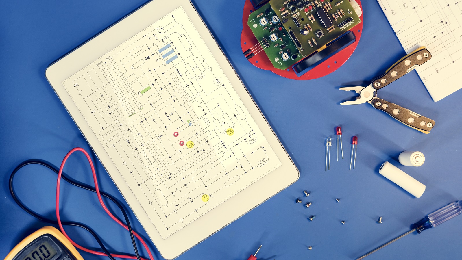
Step 2: Circuit Design Diagram
Designing the circuit using EDA (Electronic Design Automation) software; this is through the schematics, represents the drawing of the circuit specifications for interconnection of different electronic components in a feasible way. Upon completion of the schematic, the following step is PCB layout:
PCB Design Software: Draw the circuit layout using PCB design software.
Design Tips: Use copper tracks with black lines of separation between 1/100 inch and 5/100 inch. Use circles to indicate a hole drilled and size influenced by the size of the drill bit you are to use.
Step 3: Print the Circuit Layout
Print the layout on a transparent photosensitive film:
Mirror the design and flip it the right way to ensure that it comes the right way to the copper plate.
Use glossy magazine paper for best results.
Set your printer to print on the highest quality setting—some printers by default operate in economy modes that use less toner.
Step 4: Clean and Prepare the Copper Board
Proper preparation of the copper board is very important:
Clean the Board: Use a kitchen scrubbing pad and water to clean the copper surface. Get rid of all the dirt and oil.
Roughen Surface: Sand the copper surface using fine sand paper for enhanced cohesion of the photosensitive film.
Step 5: Transfer the Design for the Copper Board
The UV exposure machine is used in transferring of design:
Alignment of the Photosensitive Film: This is where the printed film is placed on the cleaned, copper part of the board.
UV Exposing: This is done by the UV exposure machine for a few minutes to solidify the non-covered section of photo-resists .
Step 6: Developing PCB
Develop the board by removing the unexposed photoresist:
Developing Solution: Develop the exposed board using sodium carbonate solution.
Rinse: Rinse the board thoroughly under water to stop the chemical action.
Step 7: Etching of PCB
Etching removes the non-circuit copper:
Etching Solution: Prepare an etchant bath by mixing hydrochloric acid and hydrogen peroxide in a plastic container.
Etching Process: Lower the board into the etching solution with plastic tongs. Periodically check on it until all the exposed copper vanishes.
Rinse: Stop the etching process by rinsing the board that has been etched.
Step 8: Removing the Remaining Photoresist
After etching, the remaining resist needs to be removed also, and to do this follow the steps below:
Strip Photoresist: Wet a paper towel with lacquer thinner and rub the board with it ever so lightly to remove the hard photoresist, exposing nice and shiny copper traces.
Step 9: Drilling Holes
Drill holes only for through-hole parts
Drill Bit: Drill holes with a high-speed steel/cobalt drill bit with proper size (usually 3/100 inch).
Drilling: Drill on the marked position carefully. It's important not to damage the board by drilling slowly.
Step 10: Optional Processes and Final Assembly
You may want to take some additional steps for added ruggedness and features:
Solder Mask Application: It shields the copper traces and prevents solder bridges.
Silkscreen Printing: Print component labels and other identifiers.
Surface Treatment: Basically, the surface of the PCB is coated with Hot Air Solder Leveling (HASL), gold plating or Organic Solderability Preservative (OSP) to improve its solderability and enable it to withstand corrosion.
Final Assembly
Component Placement: This is when we provide room for all electronic components according to layout.
Soldering: The components are held in place by soldering. It will be specific to using either a soldering iron or a wave soldering machine. It is to be ensured that the solder joints are sufficiently strong and are free from any kind of defect.
Testing and Quality Control
Before the PCB may be held as complete, the functionality of the PCB must be tested:
Electrically Testing: This can be achieved using a universal testing frame. The essence of electrical testing is that it is said to ensure that there are no electrical errors on the board and that the board works as precisely as it is designed to.
Visual Inspection: Visual inspection should be very careful in order to identify any physical defect or incomplete solder joint.
Completion and Packaging
After testing:
Final Inspection: A final check is done to ensure that the board is in order of the demanded quality standard.
Packaging: The PCB is packed in such a way that there is no damage during shipment.
Inference
Manufacturing of single-sided PCBs is quite a delicate process, from design to manufacture. With proper care and detail at each step in the process, conducted right, it results in a rugged and dependable circuit board for many applications and from simple gadgets to complex systems. Following these 10 steps to manufacture single-sided PCBs yields product of quality with efficiency and consistency.
Hot Tags:

Contact us

If you can't find what you're looking for, please contact us.
Article
PCBs (Printed Circuit Boards) are fundamental in electronics, composed of multiple layers like silkscreen, soldermask, copper, and substrate, chosen for specific electrical functions.
 2024/08/07
The article is developed concerning the breakthrough of integrated circuits and the need for custom PCBs in some electronic products. It enumerates ten golden rules in conducting PCB layout design and manufacturing: grid selection, routing, power layers, component placement, panel duplication, component value combination, frequent DRC, flexible silkscreen use, decoupling capacitors, and pre-production parameter checks. These rules provide for the optimum design and manufacturing of a PCB.
2024/07/25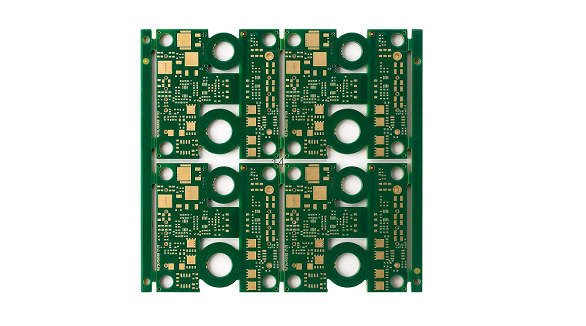
Most electronic circuits are mounted on PCBs, or Printed Circuit Boards, which provide mechanical support and electrical interconnection of electronic components. There are, however, special applications that involve the use of single and double-sided PCBs, multi-layer PCBs, or even rigid and flexible PCBs with aluminum backing, targeting medical, industrial, auto, and aerospace industries. They may use materials such as fiberglass, epoxy, aluminum, and others.
2024/07/25