How to Measure Solder Mask Thickness?
Solder masks protect PCBs from damage and solder bridging. Available in various types and colors, they ensure reliability. Eco-friendly options and precise thickness measurements are crucial for quality.
Solder mask has been playing an indispensable role in the field of PCB manufacturing. Along with shielding for copper traces, this results in reliability and long life for the PCB. In this article, one will learn what solder mask is, its importance, the different ways of application, and how to correctly measure solder mask thickness.
What is Solder Mask?
A solder mask is a liquid photoimageable lacquer applied to both sides of a PCB to protect the copper traces. This layer provides protection against oxidation, short circuits to external conductive material, soldering, high voltage spikes and a variety of environmental factors. The solder mask is sprayed onto the production panel during fabrication of the PCBs, exposed to UV light with the correct pattern and then developed and dried. Though green is the most common color used, solder masks are also available in other colors like red, blue, black, white, and clear.
Significance of Solder Mask
The solder mask plays a number of critical roles:
Protection: It protects copper traces from oxidation and environmental damage.
Preventing Solder Bridging: It serves to avoid accidental solder bridges between adjacent pads during the assembly process.
Visual Enhancement: It provides an enhanced visual contrast for better and easier inspection.
Component Placement: It aids in accurate component placement.
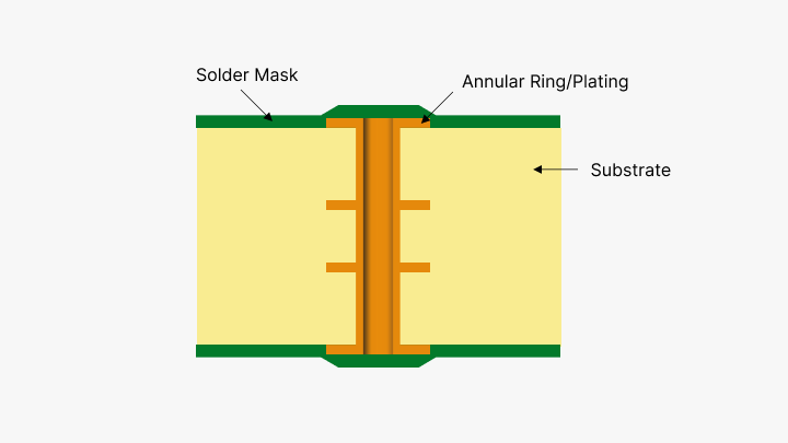
Types of Solder Masks
Several solder mask types are in use for the fabrication of PCBs, depending on the volume of production, design complexity, and cost involved:
Screen Printing: Less complex designs and lesser batch sizes fall into this category.
Liquid Photoimageable Solder Mask (LPI): Highly precise; thus, applicable to even complex and high-volume PCBs.
Dry Film Solder Mask: Very good accuracy for high-density designs.
Advances in Solder Mask Technology
With the demand for larger-scale integration of PCBs and component spacing for further functionality, solder mask technology keeps evolving. The manufacturers present advanced solder mask materials boasting better thermal resistance, improved adhesion, electrical insulation properties, and compatibility with contemporary assembly techniques, such as advanced packaging technologies.
Environmental Considerations
More recent advances in PCB manufacturing have begun to look towards ecological sustainability. This includes the majority of manufacturers moving towards solder mask materials that are considered eco-friendly using RoHS and REACH compliance, where these combined regulations minimize the usage of hazardous materials to an absolute minimum in an effort to reduce environmental impact.
How to Measure Solder Mask Thickness
Having adequate solder mask thickness is important to protect the circuit; at the same time, it also should not be too thick. Solder mask thickness needs to be measured rightly in order to keep up the quality of PCB.
Recommended Thickness Guidelines
Minimum: On top and side edges of the conductor, more than 7 microns is preferred.
Maximum: The maximum thickness for solder masks on finished copper parts up to 35 micrometers is 40 micrometers. For thicker copper, it can be up to 80 micrometers.
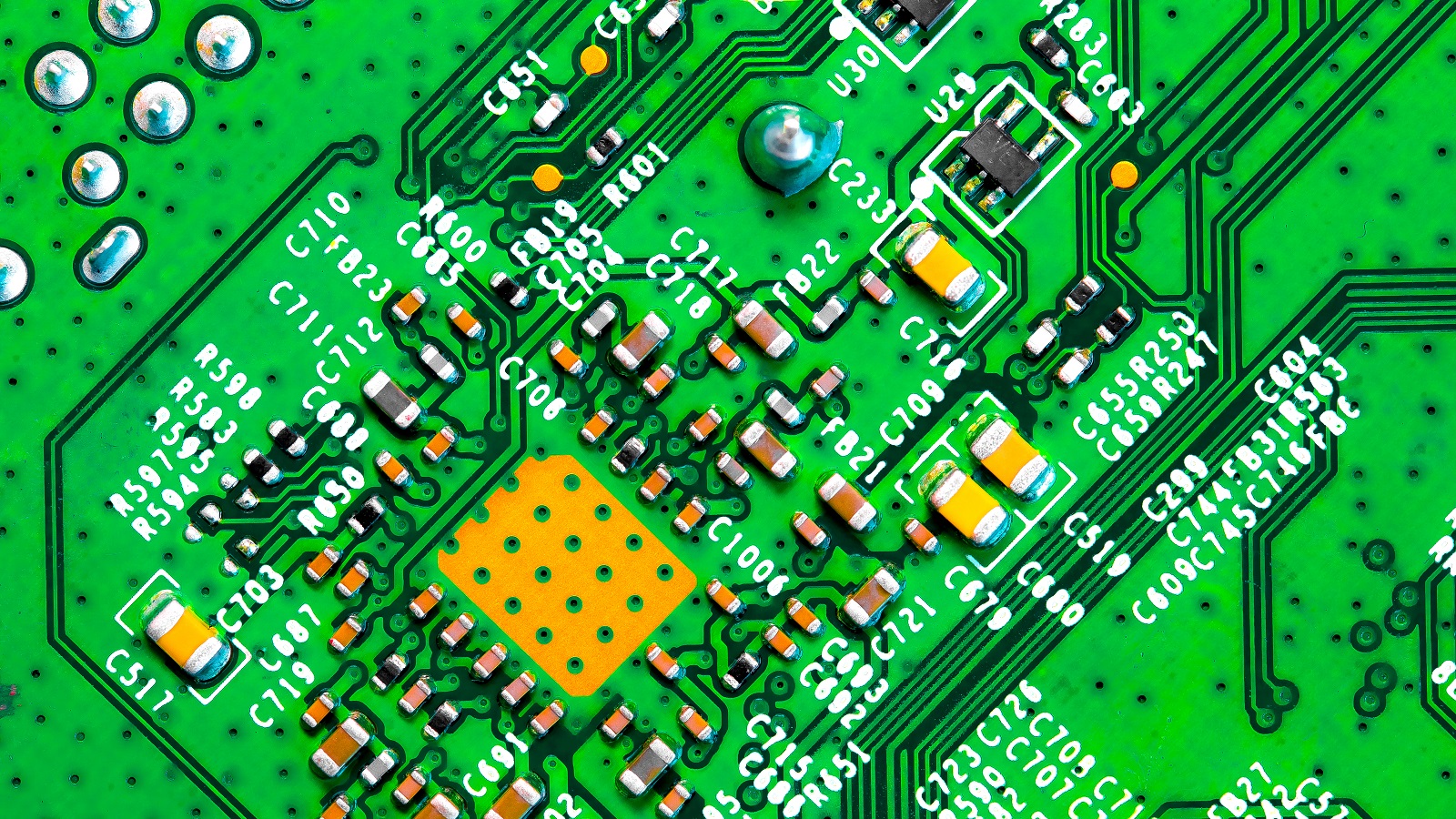
Measurement Techniques
Several techniques can effectively measure the thickness of a solder mask, which are as follows:
Microscopic Inspection: Uses high-resolution microscopes to measure the thickness directly.
Cross-Section Analysis: It involves cutting a section of the PCB and viewing it under a microscope to measure the thickness.
Eddy Current Testing: A non-destructive test was done based on electromagnetic fields that would establish the thickness of solder mask.
X-Ray Fluorescence (XRF): This is one of the advanced techniques in which changes in mask thickness are detected by using X-ray emissions.
Application Best Practices
Follow the given recommendations while application to make sure the effectiveness of the solder mask:
Annular Ring Requirements: If the solder resist is impinging on the lands, meet the minimum annular ring requirements.
Isolated Pads: Avoid leaving exposed isolated pads to avoid contamination, which may cause possible short circuits.
Plated Through Holes: Only apply solder resist on plated through holes if the design requires no solder fill.
Test Points and Connector Fingers: Avoid applying solder resist on areas such as test points and connector fingers. This is because correct testing and effective connections require bare test points and connector fingers.
Conclusion
The solder mask plays a major role in PCB fabrication for the protection of copper traces and to avoid solder bridging, thus generally enhancing functionality. Precise measurement of the thickness of solder mask is the necessary condition to assure that these masks are durable and reliable. At PCBX, we have broad expertise in every aspect of the design and manufacture of Printed Circuit Boards. Our expertise and adherence to quality ensure the production of well-designed, reliable PCBs. We adhere to the best practices of the industry and use advanced technologies to the belief that our PCBs will always meet the highest performance and reliability standards. If you have questions or need assistance, let the team at PCBX take part in your knowledge and help you achieve your goal.
Hot Tags:
Contact us

If you can't find what you're looking for, please contact us.
Article
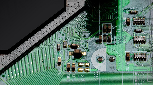
Solder mask, or solder resist, is the polymer layer on PCBs that protects against oxidation, short circuits, and solder bridges. Types include LPI, dry film, and epoxy, chosen based on design, application, and cost.
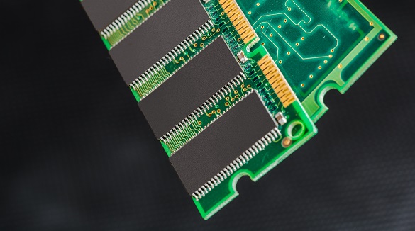
PCB thickness is crucial in electronics, influencing performance, durability, and cost. The standard thickness is 1.57mm, but other sizes exist for specific needs. Factors like copper thickness, material choice, layers, and environmental conditions determine suitability. Custom thicknesses cater to high-power, space-limited, and high-frequency applications but may increase cost and production time. PCBX offers various thickness options, emphasizing quality and customer service in PCB manufacturing.
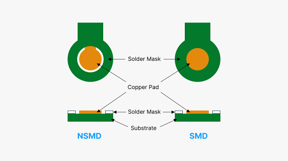
Solder masks protect PCBs from environmental damage and electrical shorts, enhancing reliability and aesthetics. The application is complex, requiring professional fabrication to ensure quality and compliance with regulations.
