How to Repair PCB Boards
PCB repair skills reduce waste and costs, ensuring durable electronic functionality by effectively diagnosing and fixing various board failures.
Printed Circuit Boards are the backbones hosting most of the essential components in virtually all electronic devices to allow electrical connectivity. Due to its important nature, malfunction or damage to a printed circuit board tends to have a great impact on the functionality of an electronic device.At PCBX, we recognize the necessity of effective and efficient PCB repair.From diagnosis to repair, this tutorial leads you through a step-by-step guide in order for you to maintain and restore these vital parts with confidence and accuracy.
Importance of PCB Repair
This PCB repair capability will be viable economically and ecologically in today's rapidly developing environment of technology.By repairing your PCBs, you minimize the costs and time wastage incurred while seeking replacements, thereby helping reduce electronic waste. Learning PCB repair skills empowers both hobbyists and professionals by improving the resilience of your electrical systems, allowing you to swiftly detect and remedy any malfunction.
Causes of Common PCB failures
The following are some of the general causes of failure that one should understand in order to properly repair PCBs:
Physical Damage to Component: Drops, collisions, and pressure are all examples of operational failures caused by physical component damage.
Improper Assembly: Misaligned components or defective parts are major reasons.
Damaged Traces: Overheating, pollution, or even unexpected power surges can cause conductive paths on PCBs to fail, resulting in signal failures.
Environmental Factors: Components might be exposed to harsh temperatures, high humidity levels, or even corrosive substances, which deteriorate them.
Static Electricity: Poor anti-static handling of the PCB will result in electrical discharge damage to the assemblies.
Thermal Overload: Components on a board may be poorly spaced, leading to overheating that results in the failure of components or charring of the PCB material.
Preparing for PCB Repair
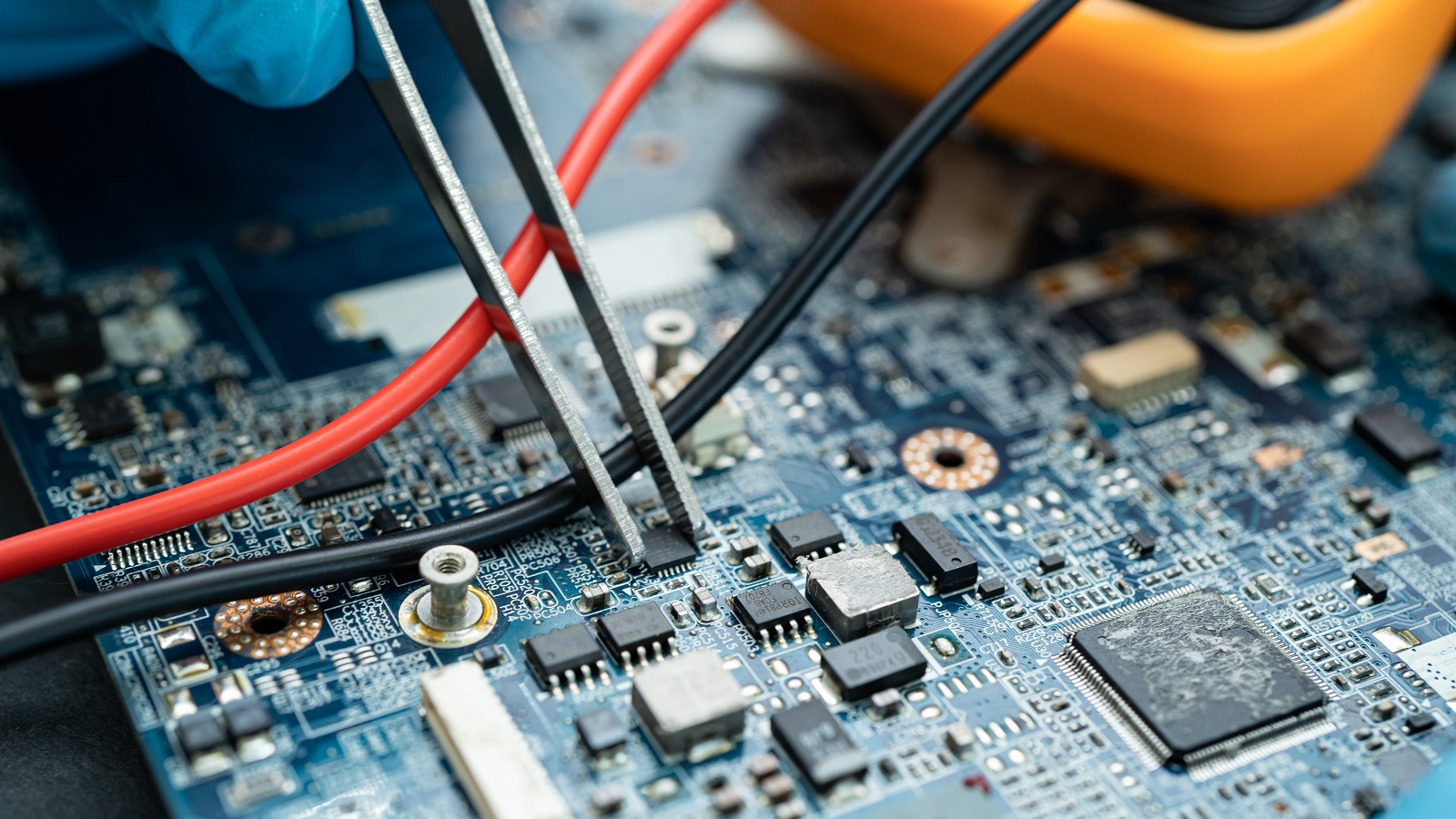
Successful repair of a PCB requires one being well suited with the right tools and materials; these are among the general ones used:
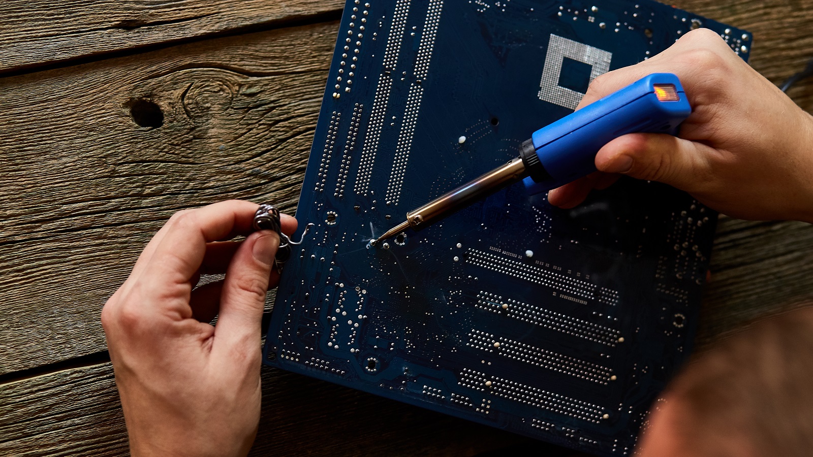
Soldering Iron and Solder: These two are important for having components fastened securely onto the circuit board.
Desoldering Pump or Wick: This acts as a suction device used in the removal of solder from the board where a component has to be replaced.
Multimeter: Utilized to test for continuity and hence very useful in diagnosing electrical failures.
Traces and small fragments are more readily observable using a microscope or hand lens.
Tweezers: used to manipulate fine components.
The flux pen is used to remove surface oxidation before soldering. You can clean boards and flux by using isopropyl alcohol. Personal and board protective gear includes safety glasses and anti-static wristbands, among others.
Step-by-Step Guide to Repair PCB
Discuss the issue: Look for any burnt marks, split traces, or damaged solder joints. Use the multimeter to check for open circuits or breaches that could indicate a problem while testing continuity of the circuit.
Remove damaged parts: Fasten the PCB onto an anti-static mat or holder so it doesn't move around. Use desolder pump or wick to safely remove the solder from the pins of faulty components. Carefully remove the parts with tweezers, being extra careful not to damage the pads on the PCB.
Repairing damaged traces: To provide a hygienic working environment, clean the area with isopropyl alcohol. If there are damaged traces, fill the gap with a thin wire or conductive pen line, then solder firmly to ensure contact.
Replace defective components: Place the new component on the PCB in the appropriate orientation for the circuit design. To increase solder flow, use a flux pen to add any needed flux. Solder the component in place using a soldering iron, ensuring that all connections are good and there is no excess solder.
Testing and Verification: Retest the circuit using a multimeter to ensure all freshly soldered components and repaired traces function properly.
To do functional testing, reassemble the board and turn the device on.
Safety Advice for Repairing PCB
Wear protective gear: Safety glasses will shield your eyes from fumes and spillage caused by solder. Protect yourself and your sensitive parts from static discharge by wearing an anti-static wristband.
Work in well-ventilated areas: Soldering produces vapors that might be detrimental to your health. Therefore, it is vital to offer excellent ventilation in the working environment.
Keep Your workstation Organized: Ensure that your workstation is clean and bright, with no clutter that might accidentally damage or dent the PCB during repair.
Troubleshooting Common PCB Issues
Short Circuits: Check solder connections for bridges and ensure that components are oriented properly. Whenever feasible, modify pad layouts to decrease the chance of shorts.
Open Circuits: To avoid circuit breakdowns, ensure that no connections are cut or damaged, and that all components are firmly soldered.
Dark or Grainy Contacts: These indicate contamination or surplus impurities in solder. Note the use of high-quality solder and proper cleaning protocols.
Golden Yellow Solder Joints: Usually caused by excessive temperature applied to the solder. There should be a temperature control always prevalent and appropriate to the component in use.
Conclusion
We firmly believe that minor details in PCB repair add not only to the life of the product but also contribute to sustainability through reduced waste. A guide like this provides all the necessary expertise for diagnosing, repairing, and maintaining PCBs for optimal performance and service life of electronic devices. Mastering repair skills-for personal projects or otherwise-is as powerful as it is practical. Even damaged circuit boards can get a second lease on life with careful handling and the right approach, and there is continuity both in function and innovation.
Hot Tags:
Contact us

If you can't find what you're looking for, please contact us.
Article
Functional testing verifies PCB functionality in simulated environments, enhancing quality and reliability, detecting faults, ensuring performance, and cost efficiency.
PCB short circuits arise from unintended connections, leading to safety risks. Prevention involves isolation, inspections, and thermal protection, ensuring device reliability and safety.
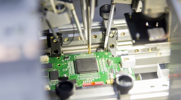
Flying Probe Testing (FPT) is ideal for low-volume PCB assemblies. It uses mobile probes and advanced features like PDM and HVS for precise, cost-effective detection of shorts and opens.
