- Products & Capabilities

- About
- Resources
Importance of DFM in PCB Manufacturing


Design for manufacturability (DFM) in PCB production ensures quality, reliability, and cost-effectiveness by optimizing component selection, placement, trace routing, materials, and testing, leading to reduced costs, better products, and faster market entry.
In the present digital era, printed circuit boards form the very backbone of virtually every electronic device. Consequently, the assurance of quality, reliability, and cost-effectiveness in their manufacturing is of prime importance. Design for manufacturability thus plays a very important role in facilitating the process of manufacturing through intelligent design-phase decisions. These decisions range from component selection to layout, material selection, to testability, in ensuring the work readiness of the PCB for manufacturing with minimal risk and delays.
Key Considerations in DFM for PCB Assembly
Component Selection
Component selection is one of the main steps for the DFM process. It is recommended that the designers chose such components that are available, standardized, and also compatible with the assembly equipment. Standard footprint components, like SOIC, QFP, and BGA, are able to interface easily with pick-and-place machinery and reflow ovens. Taking into account thermal resistance and power dissipation requirements earlier in the design phase saves costly redesigns, reduces the complexity of the supply chain, and simplifies manufacturing processes.
Component Placement
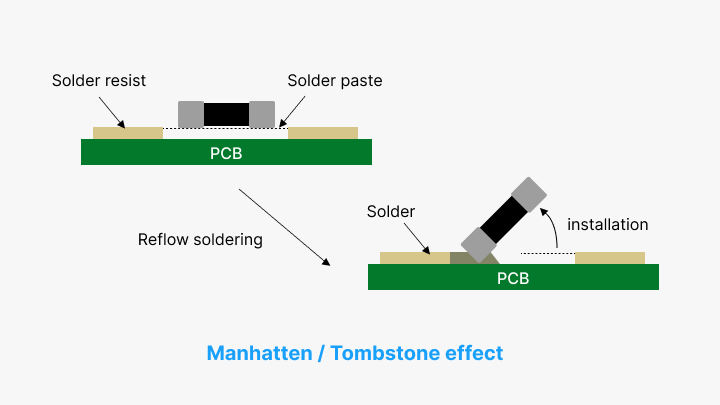
Component placement optimization is a key mandate of automated assembly and rework. Components that are too proximate to each other can result in soldering defects, such as solder bridges, and may result in difficulty with repairs. Minimum electrical clearances and creepage distances are specified so that arcing and dielectric breakdown can be avoided. For wave soldering or selective soldering, depending on the assembly method, efficient component orientation must be ensured along with suitable solder paste stencil apertures for proper, reliable solder joints.
Trace Routing
Efficient routing of traces has a big impact on both performance and manufacturing cost. Wide, well-spaced traces improve current flow and reduce signal interference. Controlled impedance routing for high-speed signals reduces reflections and preserves signal integrity. Differential pairs reduce crosstalk in sensitive signals. Appropriate trace width and copper thickness prevent voltage drops and overheating, hence increasing reliability.
Material Selection
Selection of material becomes critical in terms of both performance and manufacturability. Materials need to be compatible with different levels of assembly processes and operational environmental conditions of particular importance on thermal expansion and moisture absorption. In general, RF applications require materials suitable for operational conditions concerning TG, CTE, DK, and DF for stable and good performance. Wherever hard environments could not be avoided, protective measures such as conformal coatings or potting compounds should be implemented.
Thermal Management
Good thermal management is one of the ways of preventing early component failure and ensuring performance reliability. Design approaches will be the employment of thermal vias, heat sinks, among other cooling mechanisms in waste heat management. Thermal modeling software will be used in verifying that the temperature distribution around components at risk stays within safety limits.
Testing and Reliability
Design for testability simplifies quality control and troubleshooting. Features include boundary scan (JTAG) and BIST for automated testing and diagnostics, and accessible test points for in-circuit and functional tests for easy rework and replacement. Product reliability could be pre-determined and improved using ALT and FMEA for long-term performance and customer satisfaction.
Benefits of DFM
Reduced Production Costs
DFM reduces manufacturing cost by reducing rework rates, scraps, and manual interventions. This means lower costs per unit, easier operations, less downtime, and effective quality control and inventory management.
Faster Time-to-Market
Optimization of the whole process chain in the PCB assembly makes DFM reduce the timeline from design to production. With quicker product launches capturing market opportunities and commanding premium prices from early adopters, it strengthens return on investment and profitability.
Better Quality of Products
DFM eliminates defects, builds reliability, and reduces costly returns, repairs, or replacements. Quality products beget satisfied customers, repeat business, and positive word-of-mouth, all of which culminate in a higher CLTV.
Manufacturing Efficiency
With an optimized DFM design, there will be smoother passage through manufacturing lines, ensuring higher output and total capacity. Early identification and mitigation of hiccups reduce delays and other expensive disruptions, thus leading to more stable financial projections.
Guidelines for Inspection in DFM
Line Width and Spacing
Adherence to line widths and spacings specification is beneficial in avoiding various defects such as signal interference, crosstalk, and short circuiting. On the other hand, proper spacing will not have unwarranted etching and open circuit problems.
Hole-to-Hole and Pad Inspections
Adequate spacing between holes and pads will prevent electrical short circuiting and soldering issues. Reduced number of holes on patch pads lower the cost of the manufacturing process with increased quality of welding.
Component Packaging and Placement
Choose appropriate size components and package them. Allow appropriate clearance so that no solder bridges will occur, and manual soldering and rework are easily possible. Though smaller packages can save space, they can complicate processes of assembly and cleaning.
Check Silk Screen and Spacing
Silk screens are to be clear and accurate to avoid improper component orientation and polarity. Enough spacing between components means there is no overlap or any solder issue, especially for sensitive components like QFPs and BGAs.
Conclusion
DFM is a significant factor in every stage of the manufacturing of PCBs, right from design to assembly and testing stages. Its principles enable the selection of materials, optimization of layout, and thereby enhancement in production efficiency and quality. Since technologies are continuously evolving and market demands are also changing, the importance of DFM is an ever-increasing one. It is only when the principles of DFM are applied to their fullest that companies will be able to meet customer expectations, catch up with the competition, and attain healthy growth in PCB manufacturing. Welcome DFM to design it right, build better, and seal your place in the ever-evolving electronics market.
Hot Tags:

Contact us

If you can't find what you're looking for, please contact us.
Article
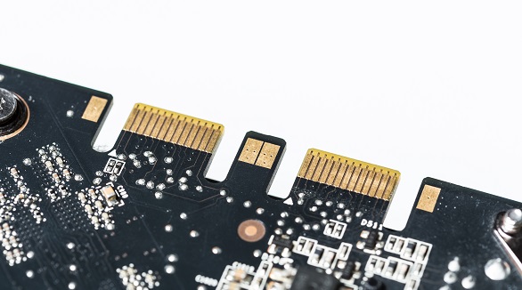
Gold fingers are essential gold-plated edge connectors on PCBs, known for durability and conductivity, crucial for transmitting digital signals in electronics. They come in Electroplated Hard Gold and ENIG types. Used in motherboards, peripherals, and industrial machinery, they adhere to IPC standards ensuring reliable, high-quality connections in modern electronic devices.
 2024/09/12
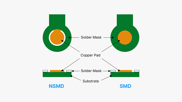
Solder masks protect PCBs from environmental damage and electrical shorts, enhancing reliability and aesthetics. The application is complex, requiring professional fabrication to ensure quality and compliance with regulations.
2024/08/20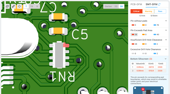
The article is developed concerning the breakthrough of integrated circuits and the need for custom PCBs in some electronic products. It enumerates ten golden rules in conducting PCB layout design and manufacturing: grid selection, routing, power layers, component placement, panel duplication, component value combination, frequent DRC, flexible silkscreen use, decoupling capacitors, and pre-production parameter checks. These rules provide for the optimum design and manufacturing of a PCB.
2024/07/25