Importance of Precision in PCB Stencil Fabrication
Precision in PCB stencil manufacturing is crucial for accurate solder paste deposition, reducing defects, and improving reliability. Key factors include material, technology, design, and maintenance.
The Printed Circuit Boards are the backbones of modern electronics, therefore providing support and connections for every other important component in a device, starting from smartphones to industrials. The application of solder paste is one of the main steps in the assembly of Printed Circuit Boards, where the quality and functionality are highly dependent on that stage. This process is chiefly carried out with the help of a stencil-a tool that provides the exact and accurate placement of solder paste on the PCB. With the pivotal nature of the stencil, high precision in the manufacture of the PCB stencil is not just a pre-requisite but an absolute necessity. This article explains why precision is important in the manufacture of PCB stencils, what factors determine the quality of the stencil, and how such precision could affect the overall performance of PCBs.
Why Precision in PCB Stencil Manufacturing Matters
Accurate Solder Paste Deposition
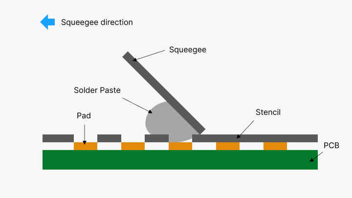
The main functions of a PCB stencil include applying the solder paste accurately to the pads of a board. High precision in manufacturing stencils ensures the solder paste is applied uniformly and to the right amount on each pad. Incorrect or variably placed solder deposition will lead to a number of problems, including:
Short circuits: Excess solder paste can bridge adjacent pads, causing short circuits that could result in the damage of the components and the board.
Open circuits: Insufficient solder paste might result in a weak or open joint, causing open circuits and unreliability.
Misalignment: Minor misalignments at times create serious effects and hamper the quality of soldering the PCB.
Precision stencils ensure the correct placement of solder paste in the required places. Precision at this point goes hand in hand with the later process of component placing. When the components fall on well-stenciled pads, they tend to fall correctly, risking no misplaced parts; hence, a better soldering quality. Precise placement of the components, particularly the fine-pitch ones like BGAs and QFNs, is highly needed. These need to be correctly aligned for the proper functioning of these components.
Consistency and Repeatability
The high precision in manufacturing processes allows the same and repeatable results on different boards. This repeatability is of immense importance, especially in high-volume assembly environments where even a minor deviation in the products may sometimes amount to huge problems. A stencil with correct aperture shapes and sizes ensures that, within a batch of PCBs, each has the same quality solder paste applied. Repeatability would mean a condition of maintaining uniformity and reducing defects to ensure high yield rates for cost savings and product reliability.
Improved Overall PCB Performance
The level of precision in the manufacturing of PCB stencils is directly proportional to the overall performance and reliability of the final product. Accurate and consistent solder paste deposition can provide stronger and more reliable solder joints, reducing field failure possibilities. Good-quality solder joints enhance mechanical stability and electrical integrity, influencing the durability and performance of the PCB and thereby the electronic device. A stencil requires high precision in its manufacturing process, especially for critical-to-reliability applications in medical devices, aerospace, and automotive electronics.

Factors Affecting Stencil Quality and Precision
Material Selection
The material used would make all the difference in quality and accuracy in a PCB stencil. Stainless steel and nickel are two of the most common materials utilized, considering their strength, flexibility, and precision in aperture dimensions even after multiple uses. Laser cutting and electroforming are the two major techniques utilized in order to create high-precision stencils from these materials.
Manufacturing Technology
Improvements in manufacturing technology have significantly improved the accuracy of PCB stencils. Among the most popular methods is laser cutting, since it provides very high accuracy and is flexible enough to manufacture very intricate aperture designs with very small tolerances. Electroforming produces highly accurate aperture walls that are uniform in nature, making this process quite suitable for fine-pitch components and high-density boards. Selection of the appropriate manufacturing process to meet the specific requirements of the PCB assembly process is important in achieving high precision.
Aperture Design and Quality Control
The design of stencil apertures would directly affect the accuracy of solder paste deposition. Included in the factors to be considered would be aperture shape, size, and spacing for optimal performance. Tight quality control, involving microscopic inspection and paste release testing, would also be required to verify the accuracy and functionality of the stencils before they see service in the assembly process.
Regular Maintenance and Handling
Even the most precisely manufactured stencils will eventually deteriorate if not properly maintained. Regular cleaning and inspection are important to prevent residue buildup that may damage the apertures. Proper handling and storage also contribute to maintaining stencil precision, since physical damage may affect the accuracy with which solder paste is deposited.
Impact of Precision on PCB Assembly and Performance
Reduced Defects and Rework
These defects are reduced by high-precision stencils, which minimize instances of rework and repair, further improving the yield rate while reducing production cost and lead time. Lower defect rates will decrease the burden of an assembly process and speed up time-to-market for electronic products.
Improved Reliability
Precision in stencil making equates to more reliable solder joints, which are crucial for both the electrical and mechanical performances of a PCB. Reliable joints minimize component field failures while enhancing the overall robustness of the electronic device, which is critical in industries where failure is never an option.
Customer Satisfaction
Quality and reliability are very important in this competitive market of electronic goods. The high-precision stencil contributes much to the fabrication of premium-quality PCBs, and these ultimately please the customers. A reliably performing product with an extended life cycle tends to enhance brand reputation and customer loyalty.
Conclusion
Precision in manufacturing PCB stencil is the most critical factor that highly influences the quality and performance of the final electronic product. Because the stencil is critical to this process, its accuracy will affect solder paste deposition, component placement consistency, and overall PCB performance. Manufacturers can produce high-precision stencils capable of meeting the most stringent demands of modern electronics assembly by paying close attention to material selection, manufacturing technology, aperture design, and maintenance. This should guarantee that high quality is attained with reliability, resulting in customer satisfaction and a stronger market position for the business.
Hot Tags:
Contact us

If you can't find what you're looking for, please contact us.
Article

Solder masks protect PCBs from damage and solder bridging. Available in various types and colors, they ensure reliability. Eco-friendly options and precise thickness measurements are crucial for quality.

PCB panelization consolidates multiple PCBs into a larger board, improving manufacturing efficiency and reducing waste. Techniques include V-scoring and tab-routing. Proper design enhances assembly, testing, and cost-effectiveness.

PCBs are essential for electronic devices, providing mechanical support and electrical connections. This article explores the importance of PCB panel dimensions, standard sizes, and optimization techniques. Key points include cost-efficiency, ease of manufacturing, quality control, and optimal layouts. Factors like board size, volume needs, and equipment capabilities influence panel size. Coordination with manufacturers, using design software, and employing standard sizes can enhance production efficiency and quality.