In-Circuit Testing (ICT)
In-Circuit Testing ensures PCB reliability by verifying component integrity and connections, with advantages in accuracy and coverage, but high setup costs.
In the complex world of manufacturing for PCB assemblies, ensuring functionality and reliability are crucial success factors for electronic devices. In-Circuit Testing, a thorough testing methodology that verifies the integrity and functionality of individual components and their interconnections on a PCB, has a very important role in this process. The process of ICT testing not only reduces early defects in the production process but also maintains overall reliability and quality expected in finished electronic products.
In-Circuit Testing is a very accurate test applied to check operation on PCBs with the help of special test equipment called ICT testers. These testers use a set of electrical probes to contact the PCB test points to measure parameters like resistance, capacitance, and signal integrity. The tight process makes sure that each component on the board operates within pre-set parameters, and hence defects such as short circuits, open circuits, wrong value components, or faulty solder joints are highlighted efficiently.
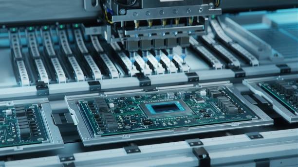
How Testing Works with ICT
In achieving this, the process of ICT is based on a sequence of steps that have been cautiously laid down to ensure that every electronic component on each PCB will work without fault. Let me look at how ICT testing works:
Test Fixture Setup: The PCB then goes into a custom test fixture which fixes the board in place and aligns it correctly with the probes used to test. This setup is highly critical; proper measurement depends on this, as well as consistency.
Program Loading: A particular test program is loaded into the ICT system, which is generated to meet the particular design of each PCB and components making it up. It contains test sequences and parameters that are needed for complete scrutiny.
Power Application: The application of power to the PCB for functionality would be in conditions that have been simulated similar to when it would actually be in use. This allows for effective functionality of the components to be evaluated in natural operating conditions.
Electrical Connection Testing: The system will check the PCB's connectivity by contacting the test probe with various test points to make sure accurate signal paths are made and detects open circuits or broken connections.
Component Verification: All components are tested individually with the purpose of checking if they fall within specified electrical parameters-resistance, capacitance, and inductance-that validate their integrity and performance.
Functional Testing: This is the checking of operational performance by the PCB to see whether the output signals are correct and whether the circuits perform according to the designed specifications. This step further advances the work of the board in real time operation, confirming its overall performance.
Data Collection and Analysis: ICT testing also covers data collection and analysis, which is done in much detail in real time. Advanced software tools conduct automated analysis and can pinpoint any discrepancies or faults immediately, thus providing feedback in no time.
Fault Diagnosis and Reporting: Once a fault is detected, the ICT system produces comprehensive diagnostic reports showing location and nature. This information is invaluable in the identification of the problem and aids in speedy repairs.
Re-testing After Repair and Final Quality Check: Once the faults identified have been corrected, the PCB is put once more to testing. Final quality checks entail confirmation that the PCB is to specification without defects and hence fit for distribution.
Advantages of ICT
ICT presents a host of advantages which make it indispensable in the field of electronic manufacture to wit:
High Accuracy and Speed: Speed and accuracy with which the defects can be correctly detected make ICT indispensable when volume productions are concerned.
Extensive Fault Coverage: There is great exposure in ICT to a wide number of defects that one could find on a board, thus allowing the manufacturer to deal with myriads of issues systematically.
Easy Use: The simplicity of setup and operations of systems using ICT contributes to reduced user errors and improved reliability.
Flexibility: ICT systems can easily accommodate most types of PCB design without any problem and are readily updated for more current testing techniques or methodologies as they emerge, so that even evolving technologies would keep them useful.
Challenges and Limitations
Despite its many strong points, ICT does face a number of challenges:
High Fixture Costs: In-circuit test fixture generation is generally an investment; the initial costs are such that they often tend to be highly prohibitive for lower volumes of production.
High-Density Component Testing: With ever-denser PCBs using ever-smaller surface-mounted components, good contact with tightly packed test points may problematize ICT in practice.
Requiring Regular Maintenance: The systems need periodic cleaning and, above all, replacement of the test probes in order to deliver their results with full, true accuracy.
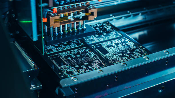
While most electronic products become increasingly sophisticated and compact, In-Circuit Testing remains a standard method of testing PCB boards. Helping to ensure each component and every connection on a board functions correctly, ICT enhances product reliability at final assembly and testing. We are committed to the application of state-of-the-art ICT systems at PCBX, ensuring our products meet the best-in-class performance and dependability standards-a commitment keeping pace with the latest developments in technology at PCB manufacturing.
Hot Tags:
Contact us

If you can't find what you're looking for, please contact us.
Article
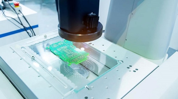
As PCBs and components shrink, AOI (Automated Optical Inspection) replaces visual inspection in SMT assembly, ensuring high-quality solder joint performance through intelligent, optical techniques.
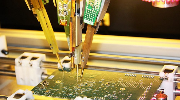
Flying Probe Testing ensures high-performance, durable PCBs and PCBAs by detecting issues like shorts and capacitance mismatches, speeding up production, and reducing costs.
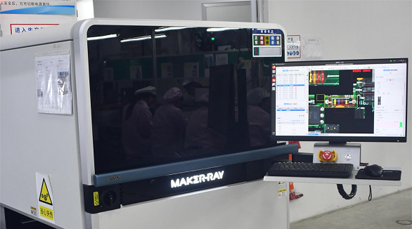
These SMT PCB assembly methods are involved, ensuring that several defects are detected. This includes the use of Automated Optical Inspection, In-Circuit Testing, and Automated X-ray Inspection. The combination of these methods is beneficial in facilitating an optimal inspection process.