- Products & Capabilities

- About
- Resources
Inspections and Tests Applied in the SMT Assembly Process


With SMT assembly at the forefront of electronics manufacturing, advanced inspection technologies like visual, AOI, ICT, and X-ray are essential due to increasing component complexity. Inspections throughout all stages—incoming, process, and post-reflow—address defects, ensuring quality and reducing rework.
With SMT assembly being the primary technology in current electronics manufacturing, new materials, technologies, and equipment will be developed indefinitely. This is consistent with the ever-increasing assembly density, an increasing number of pins, and decreasing pitch diameters. Furthermore, more and more SMDs are packaged with visionless pins.
These developments have raised scrutiny and test demands in the SMT assembly process. There is a growing need for careful development of inspection and test procedures coupled with the selection of suitable inspection technologies.
SMT Inspection and Test Technology
Among others, some of the usual techniques applied in inspecting and testing during the SMT assembly process are visual inspection, AOI, use of X-ray, and ICT.
Visual Inspection
The name implies that visual inspection involves staff inspecting product quality against manufacturing standards with their naked eyes. This method is widely used since it is simple to use and inexpensive, but its accuracy is strongly dependent on the staff's expertise and attitude. However, due to physical limitations, visual inspection is not able to inspect 0603 or 0402 packages and some fine-pitch components. Visual checks in the SMT manufacturing line normally occur after solder paste printing, before reflow soldering, and after reflow soldering. Of these, the one before reflow soldering is the most critical.
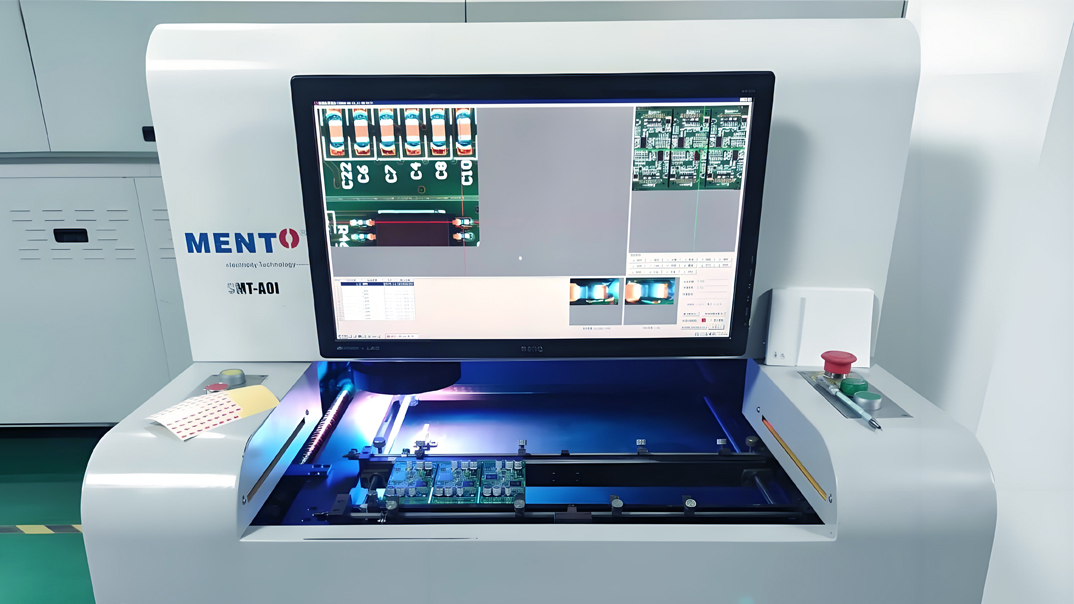
AOI
AOI normally makes its foray right after post-reflow visual inspections to identify the defects with the help of high-speed and high-accuracy Optical technology. The AOI machine captures images of the targets it inspects and does a comparison with predefined parameters stored in a database to mark PCB defects.
Finally, AOIs include simple programming and operations. The approach, however, cannot be used to undertake structural inspections on components with visionless solder connections, such as Ball Grid Arrays. Furthermore, AOI cannot detect hidden problems like as component or PCB warpages.
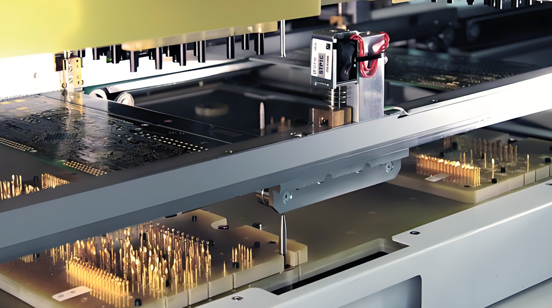
ICT
ICT normally utilizes flying probe testers and bed-of-nails testers to test modules right after SMT assembly. The electrical performance of the PCB's components can be tested, and ICT can discover improper circumstances such as missing, incorrect, or damaged components, shorts, opens, and assembly problems.
X-ray Inspection
X-ray inspection checks the quality of the solder joints by scanning the PCB. Because of X-rays' penetrating capacity, the quality of soldering could be seen in great detail. Compared to AOI, the technique of the X-ray inspection could let out more dimensions of the solder joints; however, this is more expensive.
SMT Inspection in Placement Settings
Inspections happen at all levels while the sub-assembly process of the SMT progresses—from acceptance of the raw materials to completion of the same assembly.
Pre-assembly Incoming Inspection
The incoming inspection process mainly monitors the quality of all the materials used for SMT assembly, from PCB bare boards to stencils, components, and solder paste.
Process Inspection during SMT Assembly
Process inspection during SMT assembly tests the performance, and identifies, and addresses the defects emerging from the solder paste printing, chip mounting, and reflow soldering.
Module Inspection and Rework after Reflow Soldering
In the end, the quality of reflow soldering and the functionality of the assembled module are checked for defects, and rework measures are taken.
Incoming Inspection
The incoming inspection includes bare boards of PCBs, components, and solder paste.
PCB Bare Board Inspection
Size and Appearance: Size inspections include checks for aspect ratio, space, tolerance, and size related to the edge of the PCB. The appearance inspections are targeted inside/outside layers of multi-layer and single/double-sided PCBs. Such inspections look for open, short, scrape, line width, tracing, and other flaws.
Warpage: Warpage is measured by pressing corners of the board to a surface and measuring the distance from the fourth corner to the surface.
Solderability: Checks pads and electroplated through holes using edge dips, rotation dips, wave dips, and solder ball tests.
Internal Defects: Techniques like microsectioning inspect internal defects such as the thickness of copper, conductive layers' alignment, and integrity of lamination.
Component Inspection
This is an orbital inspection procedure in which elements are evaluated for performance, specifications, package, order requirements, product reliability, assembly technique, and storage. Lead coplanarity and layer thickness are also checked to assure technological compatibility and thermal endurance.
Solder Paste Inspection
Qualified solder paste should contain 85%-92% metal content, curing strength, and adhesion from 200 Pa·s to 800 Pa·s.
In-Process Inspection
The primary procedures involved in SMT assembly include solder paste printing, chip mounting, and reflow soldering. The entire process should be inspected to guarantee a high pass rate; quality checks need to be done immediately after every fundamental process to detect defects at an early stage. Some of the processes detailed above include:
Solder Paste Printing Inspection
The standards are:
The solder paste is well distributed
Correct alignment with pads in size and shape
Correct solder quantity and thickness
Molded solder paste with no collapse or cracks
Adequate coverage area
Chip Mounting Inspection
Chip mounting defects include misplacement, missing parts, excessive glue, incorrect parts, wrong direction, floating, and rotation. With the occurrence of said defects, an immediate parameter adjustment is necessary.
Reflow Soldering Inspection
Common defects are tombstones, insufficient solder, oxidation, void soldering, solder balls, and cold soldering. Each of these qualities requires correct rectification to ensure appropriate soldering procedures do exist.
Product Inspection and Rework
Product Inspection
Following the SMT assembly process, items must undergo ICT and functional testing. The flying probe tester is one of the most often used pieces of ICT equipment today. This test equipment uses probes instead of a nail bed fixture and can record tests straight from CAD software. This improves flaw detection accuracy.
Functional tests performed after ICT evaluate the system's adherence to design specifications. The system is powered by input signals, and the output signals produced are examined to ensure that they match the functional indices.
Rework
Modules that fail to qualify are subject to manual or station rework. In the case of manual work, sophisticated tools, and skillful people will be required. On the other hand, professional rework stations are required in the case of complex PCBs.
Chip Component Rework: Correct tombstones, insufficient solder paste, shorts, misplacement, and cracks by providing accurate manual adjustments and refilling the solder paste.
IC Component Rework: This includes bridging, inadequate tin, and displacement repairs; most of the time, the components must be removed and resoldering manually.
Manufacturers can reduce rework occurrences and boost product pass rates by implementing rigorous inspection and rework processes.
Hot Tags:

Contact us

If you can't find what you're looking for, please contact us.
Article
Ensuring BGA soldering quality involves defect prevention, pre-soldering measures, and precise control during SMT assembly and reflow soldering.
 2024/08/20
As PCB lines and components shrink, traditional visual inspection fails; AOI using DRC and CAD methods is crucial for quality SMT assembly, offering intelligent, accurate inspections.
2024/08/08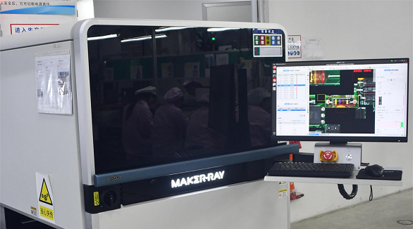
These SMT PCB assembly methods are involved, ensuring that several defects are detected. This includes the use of Automated Optical Inspection, In-Circuit Testing, and Automated X-ray Inspection. The combination of these methods is beneficial in facilitating an optimal inspection process.
2024/07/26