- Products & Capabilities

- Simulation Design & EDA

- About
- Resources
Introduction to PCB Copper Plating


PCB copper plating is key for creating conductive traces that drive electronic circuits, offering benefits like conductivity, anti-corrosion, and cost-effectiveness. Plating methods include electroless and electrolytic.
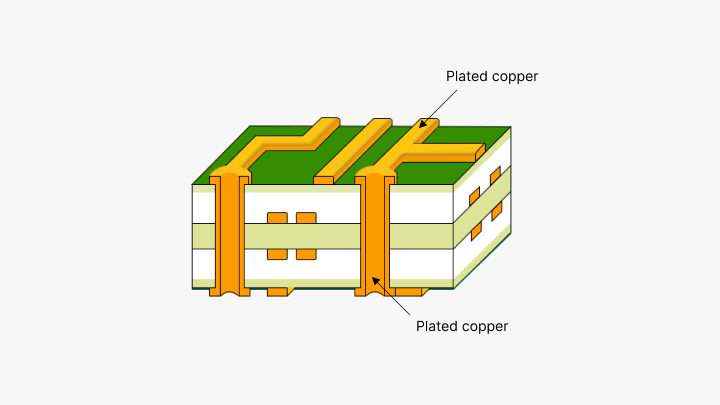
PCB copper plating is the highly crucial process of putting a thin coating of copper onto the substrate of a printed circuit board. The copper layer functions as the conducting channels or traces that allow electrical current to pass across it, and so serves as the backbone for an electronic circuit's operation.
Why Copper is Used in PCBs?
Copper is used in the fabrication of PCBs for the following reasons:
Very Good Electrical Conductivity: Copper, at a value of 5.96×10⁷ S/m, allows better current flow and forms the core of many high-frequency and high-speed operations.
Anti-Corrosive: Copper naturally forms a patina upon exposure in air that protects the metal from further corrosion.
Solderability: Copper is easily alloyed with a tin-lead solder, which results in strong and reliable solder joints.
Thermal Conductivity: Excellent thermal conductivity provides efficient heat dissipation and prevents excessive thermal buildups.
Ductility: Copper can be rolled or pressed into thin sheets, suitable for laminating onto PCB substrates.
Cost-Effective: Compared to other conductive metals such as gold or silver, copper is less expensive, making its use feasible for all kinds of PCB productions.
Methods of Copper Plating on PCB
There are a number of methods currently in practice for depositing copper onto PCB substrates:
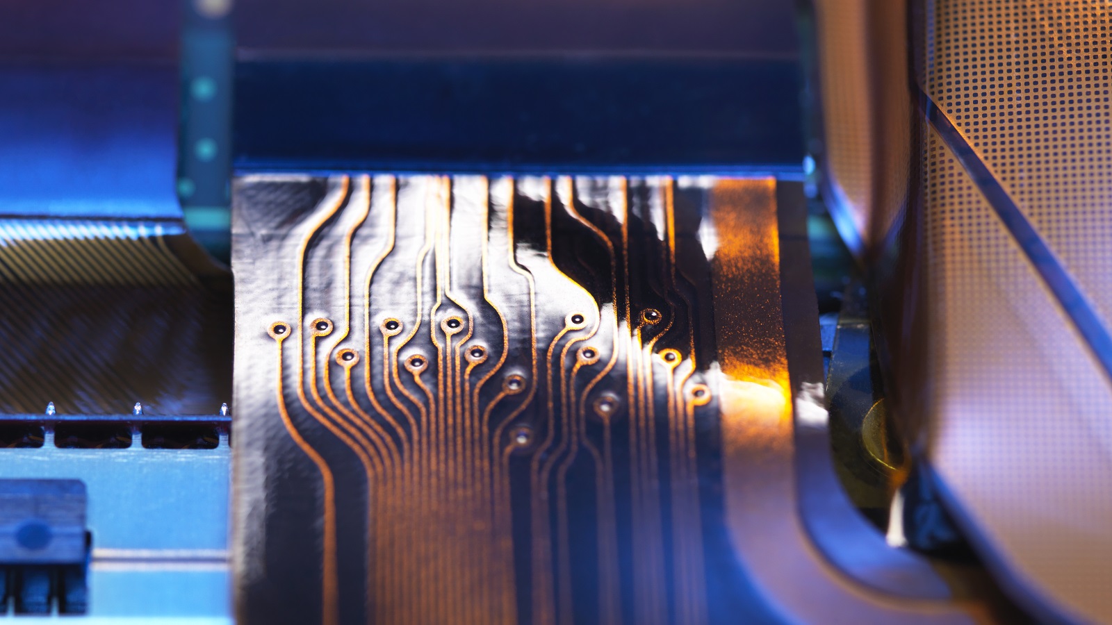
1. Electroless Copper Plating
This is an auto-catalytic process that deposits the first thin layer of copper on non-conductive surfaces without an external power supply. More precisely, the board is immersed in a copper solution, which, by means of a chemical reaction, deposits copper onto the surface. This basic layer is usually 0.1-0.5 μm thick and may then undergo subsequent electrolytic plating.
2. Electrolytic Copper Plating
This process, on the other hand, refers to the deposition of copper ions onto an electrically conductive substrate from a copper electrolyte solution using electrical current. It can give very accurate copper thickness by adjusting current and plating time up to 70 μm.
Steps in the Copper Plating Process of PCBs
The general sequence of steps in copper plating onto a PCB are given below:
Drilling: This process is done for creating through-holes as per the circuit design.
Deburring: Smoothening out rough edges and removal of drill debris.
Cleaning: Alkaline cleaners remove oils, resins, and debris.
Activation: Microetching, predip chemical treatments.
Electroless Copper: Deposit initial, very thin copper layer.
Panel Dry Film: Laminate and image a photoresist dry film.
Electrolytic Copper Plating: Plate bulk copper to thickness spec.
Strip Resist: Remove dry film to reveal copper pattern.
HAL & OSP: The application of hot air leveling and organic surface protectant.
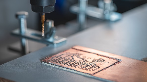
Etching: This process removes unwanted copper, leaving the desired traces and pads.
Soldermask & Silkscreen: Insulation of copper surfaces and printing of labels.
Hot Air Solder Leveling: Reflowing and leveling of the copper surface.
Final Finish: Applying finishes such as ENIG, Immersion Tin, or HASL.
Electrical Testing: Ensuring that the product is correctly functioning before assembly.
Importance of Good Copper Distribution
Good copper distribution is required to have a reliable functioning PCB. Some of the issues that need to be addressed are: filling for ample current-handling capability, placement of ground planes to provide for noise shielding, ensuring clearances with no shorting of signals, balancing copper weights, and verifying global current density in order to avoid defects and to optimize the plating rate.
PCB Copper Plating Defects
Some common defects include:
Pitting: Small holes due to impurities.
Nodules/Protrusions: Bumps due to high current density.
Orange Peel: Inadequate agitation of solution causes a coarse texture.
Plating Voids: Air bubbles create an absence of deposit.
Dull/Burned Deposits: Black and rough surfaces due to high rate of plating.
Cross Panel Variation: Non-uniform current leads to variations in thickness.
All these defects are reduced by good process control and optimized parameters of plating.
Environmental Considerations
Copper plating generates wastewater that is heavily laden with metals. The treatment methods in order of the best include counterflow rinsing, copper recovery with ion exchange resins, chemical precipitation, bacterial decomposition, and advanced treatments such as ozone oxidation and zero liquid discharge methods.
Trend in PCB Copper Plating
Among the new developing trends is the use of:
Direct Metallization: Inkjet and aerosol jet printing.
Pulse Plating: Uniform deposit and less stress in copper.
Advanced Sensors and Additives: Optimizing distribution in plating and giving better adhesion in copper.
Specialized Plating: Into HDI microvias for enhanced reliability.
Conclusion
PCB copper plating is one of the major processes in constructing conducting circuitries. Both electroless and electrolytic techniques provide ways to apply copper due to its high conductivity, resistance to corrosion, inexpensiveness, and solderability. Distribution as needed, defect control, and adherence to all relevant rules and environmental regulations take critical importance in high-reliability PCBs. Innovative trends keep up the pace in further development and enhancement of the copper plating process as modern electronics place much higher demands on density and reliability.
Trust the high quality of PCB copper plating and reliable solutions for PCBs by PCBX, with leading industry expertise and technology. Please do not hesitate to contact us regarding your PCB needs.
Hot Tags:

Contact us

If you can't find what you're looking for, please contact us.
Article
Etching is crucial in PCB production, removing unwanted copper to create conductive pathways. Techniques include chemical, laser, plasma, and photochemical etching, each with advantages and limitations ensuring PCB performance and reliability.
 2024/09/24
Gold plating in PCB manufacturing increases electrical properties, durability, and corrosion resistance, ideal for high-reliability applications. Types include ENIG (common, flat, solderable) and ENG (thicker, durable).
2024/09/20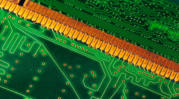
PCB side plating, or edge plating, involves copper along PCB edges, enhancing connectivity, conductivity, shock protection, and assembly, especially for small boards. Used in Wi-Fi and Bluetooth modules, it improves signal quality and EMC. Limitations include necessary design gaps and exclusion of V-cuts.
2024/08/21