Introduction to Surface Mount Technology (SMT Assembly)
Surface Mount Technology (SMT) revolutionized electronics, facilitating smaller, faster, and more reliable products. It mounts components directly on PCBs, enabling miniaturization and automation. Though SMT boosts space efficiency, cost-effectiveness, and reliability, it poses rework challenges and requires high initial investment.
The major goals of the electronic industry are efficiency, precision, and miniaturization. Surface Mount Technology plays an extremely significant role in meeting these demands. In changing the way of manufacturing of any electronic device, SMT revolutionized it to a method by which we could create smaller, faster, and more reliable products. The article will introduce the SMT process, its features, advantages, and disadvantages to get an overview of this very important technology.
What is Surface Mount Technology?
SMT is an electronic assembly manufacturing technique whereby the electronic components are mounted directly onto a PCB. This technique differs from conventional TH technolo- gy in that instead of passing component leads through holes in a PCB, SMT components come with small metal tabs or end caps, which are directly soldered onto the board's surface. This method enabled more compact, densely populated circuit boards and automated many of the assembly processes associated with them, thus shortening production time while increasing productivity.
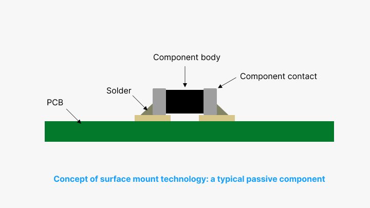
The SMT Process
The SMT manufacturing process contains some crucial steps that ensure the electronic components are accurately and reliably placed onto the Printed Circuit Boards. These are as follows:
Solder Paste Application
Solder paste is a mixture of powdered metal solder and flux applied to the PCB via a stencil. A stencil will ensure the correct placement of the paste onto the solder pads where the parts will be placed. Proper application is important to develop good electrical connections during the reflow soldering stage.
Component Placement
After applying solder paste, the PCB moves into the component placement phase. The SMDs are picked and placed onto the PCB by specialized pick-and-place machines. These machines work very fast and are also very accurate, placing generally thousands of components per hour.
Reflow Soldering
After component placement, the PCB enters a reflow oven. By ramping up temperature, it flows the solder paste to create solid connections between the components and the PCB pads. The whole process is divided into zones in order to enable the optimal solder joint formation without damaging the components.
Inspection and Testing
After reflow soldering, the assembly goes through stringent testing. Mostly, this will be done with AOI and X-ray inspection systems, which faultlessly bring out faulty areas like misaligned components and poor joints to show poor performance or unreliability in the end product.
Features of SMT
SMT has a number of features that distinctly set it apart from conventional thru-hole technology. They include the following:
Miniaturization
SMT facilitates the use of much smaller components, unlike through-hole technology. These small components can be placed very near to each other, thus achieving greater density of the placement of components in a PCB. This miniaturization is very important for compact electronic devices and lightweight devices.
Better Automation Process
The accuracy and speed of the pick-and-place machines automate the manufacturing process. Automation increases production rates, minimizes human error, and enhances consistency across batches.
Higher Frequencies and Performance
The shorter electrical paths reduce signal interference and permit higher frequency operations. Performance improves, more so in high-speed and high-frequency devices.
Better Thermal Performance
More components coming directly in contact with the PCB aid in dissipating heat more effectively. This consequently boosts the thermal performance and reliability of the electronic assembly.
Advantages of SMT
Understanding the benefits of SMT will shed light on reasons as to why this is currently the most extensively used technology in electronic manufacturing:
Space Efficiency
Due to the two-sided mounting of components in a PCB, this is the best-in-class space economy. This indeed matters toward shrink size and mobility of products.
Cost-Effective
The technology is automated. As a result, it involves only the limited requirement of labor. Large numbers of holes are drilled earlier in an attempt to mount the components on the board. It also involves manual soldering. This is beneficial in terms of cost effectiveness in the production process on the count that it reduces man-hour as well as saved time or resources.
Improved Reliability
Total product consistency and reliability are ensured with automated assembly processes, which definitely minimize the chances of human error. Automated inspection and testing lead to better quality of final assemblies.
Flexibility in Design
SMT can support a number of different types and sizes of components, providing flexibility in design to produce complex and innovative electronic devices. The flexibility in production is also attributed to the fact that either side of the PCB can be used for SMT.
Disadvantages of SMT
Though SMT has so many benefits, it, however, does not come without a challenge or limitation:
Difficulty in Rework and Repair
SMT components are mounted on the circuit board in a small scale dimension, and they are closely packed onto the PCB, so it becomes somehow difficult to rework or repair. The need for specialized equipment and experts is frequent in the circumstance.
Initial Investment
Setting up an SMT line of production is an extremely upfront expensive process in terms of equipment and technology. It involves pick-and-place machines, reflow ovens, and inspection systems. Although this investment can be offset by its long-term benefits, it still poses a barrier to the smaller manufacturer.
Mechanical and Environmental Stress
SMT components can be several orders of magnitude more sensitive to mechanical stress, such as vibration or impact, compared to through-hole versions. Similarly, the harsh operating environment, such as thermal conditions and humidity, has an effect on the integrity of the solder joints.
Design and Manufacturing Complexity
SMT requires both design and manufacturing accuracy. Any mistake, such as improper solder paste application or a misaligned component, will lead to defects difficult and time-consuming to correct.
Conclusion
Surface Mount Technology has come a long way in driving the whole scenario of electronic manufacturing and ultimately caused smaller, faster, and more reliable devices. Efficient use of space, compatibility with automation, and better performance over traditional methods make it the technology of present and future.
The advantages attached to SMT are immense, though superseded by other challenges such as the high initial investment associated with investment and repair complexity. Thus, despite electronic development, SMT will continue to remain important in innovating new ways that bound to push the limits of what can be achieved in technology design and application. Knowledge on the SMT processing, characteristics, strengths, and weaknesses equips an engineer or manufacturer with the abilities and knowledge required to really exploit the given technology and underpin the future world of electronics.
Hot Tags:
Contact us

If you can't find what you're looking for, please contact us.
Article
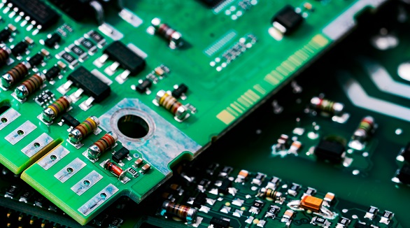
Printed Circuit Board Assembly (PCBA) employs Through-Hole Technology (THT) and Surface Mount Technology (SMT). THT offers robust mechanical bonds, ideal for high-stress applications, whereas SMT supports efficient, high-density assemblies. Each method has unique advantages and limitations, impacting cost, manufacturing efficiency, and component compatibility. Understanding these differences is key for optimal PCB design.
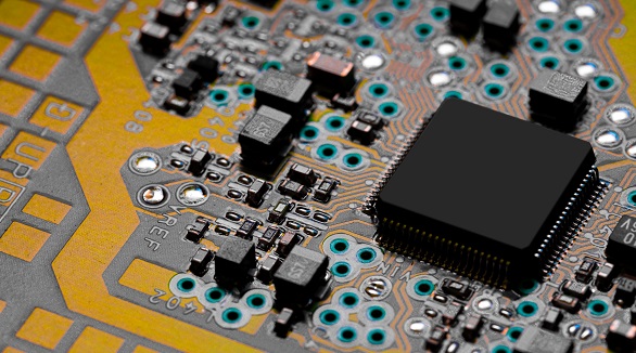
The article introduces the SMT (Surface Mount Technology) assembly process and future trends. Key steps include solder paste printing, chip mounting, reflow soldering, cleaning, inspection, and rework. Future trends highlight fast, flexible systems, green practices, and high-efficiency, intelligent systems. SMT's potential revolutionizes electronics manufacturing with wide industrial applications.
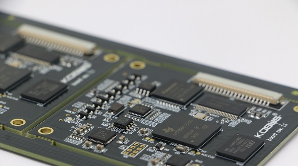
SMT assembly places components directly on PCBs, enhancing miniaturization, performance, and efficiency. Key steps: solder paste printing, chip mounting, reflow soldering, and inspection.
