- Products & Capabilities

- Simulation Design & EDA

- About
- Resources
Key Difficulties and Tips for Backplane PCB Fabrication


Backplane PCBs support functional boards, distribute power, and transmit signals. Increased IC complexity demands more layers and high performance, creating challenges in alignment, drilling, electroplating, ICD issues, and stub management. Tips include precise alignment control, advanced drilling and plating techniques, and maintaining stub lengths below 0.25mm for optimal signal quality.
A backplane printed circuit board, for most laymen, is simply a baseboard to connect the other functional boards, and able to host any one of its daughterboards or even line cards. Besides subboard accommodation, it is mainly for distribution of power to the functional boards and the loading of electrical connections and signals. Consequently, there is a symbiotic relationship: the functionality of the system is achieved by both the backplane and the subboards.
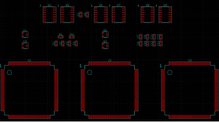
Backplane boards now serve more purposes than just supporting functional boards; they also transmit signals and distribute power as IC products become more complex, have more I/O, and are capable of high-frequency signals and high-speed digitizing due to advancements in electronics assembly. Under this circumstance, backplane boards are required to having more layers to cater to all these functions. There will be strict requirements for the layer counts, which can vary from 20 to 60 layers, board thickness from 4 mm to 12 mm, via count from 30,000 to 100,000, and also reliability, frequency, and quality in transmitting signals.
To achieve the above performance requirements, backplane PCB fabrication needs to overcome the incredible challenges, involving board thickness, board size, layer count, alignment control, back drilling depth, and stub management. This article tries to give a detailed introduction on core problems during the backplane PCB fabrication process and how to deal with them from over a decade's experience in fabrication at PCBX.
Alignment Control
Alignment control is one of the main problems in the creation of ultra-multi-layer PCBs because misalignment usually causes shorts. However, there are a lot of processes and problems that affect alignment control, with layer stack-up being the most important. Three general types of stack-up in multi-layer PCB are: mass-lam, pin-lam, and heating thermocouple.
Tips:
- That is because it seldom creates a shock effect on the core board.
- In cases where pin-lam is simply not a possibility, copper-iron rivets along with small dowels can be used.
- In the pin-lam stack-up, the type of pins should be carefully selected based on their binding abilities. In several samples, four pins performed better than eight circular pins, even though some alignment controls were required in some studies.
Drilling Technology
A backplane board is relatively thick, and hence, it is difficult to drill. Short tools are not long enough for the hole to pass through the board, and long tools are too thin and can be very easily broken while drilling; at the same time, large quantities of dust may block the hole so that the tool itself breaks. During this period, burrs might form at the hole, which will seriously affect the performance of the backplane PCB.
Tips:
- The CCD method is used in drilling backplane boards. The CCD markers are determined by the holes already drilled using X-ray drilling.
- Conductive depth control methods can accurately control the drilling depth.
Electroplating Capability
Due to the high thickness of backplane boards, the aspect ratio is typically large. Thus, there will be a need to ensure the presence of an adequate amount of copper deposited inside the holes. If not enough, it may lead to an uneven distribution of copper in the hole and will affect the via apertures and hole wall copper thickness compatibility.
Tips:
- Compare plating solutions between pulse plating and DC plating in order to find out the plating capability, reliability of the deposit, and solution stability.
- Use advanced DC plating solutions, such as EP.
ICD Analysis
High-frequency materials may create electrical connections and later long-term reliability and quality risks from inter-layer dielectric (ICD) issues. The root cause of ICD difficulties should be identified, and remedies developed to eliminate them in high-frequency material backplane PCB production. The main causes of ICD difficulties are resin gel residue on inner copper layers and poor cleaning techniques.
Tips:
- Verify the degree of aging of board materials to avoid bonding inner copper layers with insufficiently aged resin.
- Optimized drilling parameter controls for proper gel removal.
Backdrilling Stub
At high speed, stubs would lead to distortions or even a total failure in transmission, which should be taken account. According to the studies, if the stub length is smaller than 0.25 mm, its effect on the signal is minimal and can thus be ignored. So, the length should be limited to the greatest outcomes.
Tips:
- To ensure less deterioration of signal transmission quality, stub lengths should be consistent and remain below 0.25 mm.
Hot Tags:

Contact us

If you can't find what you're looking for, please contact us.
Article
Flying Probe Testing (FPT) is ideal for low-volume PCB assemblies. It uses mobile probes and advanced features like PDM and HVS for precise, cost-effective detection of shorts and opens.
 2024/08/01
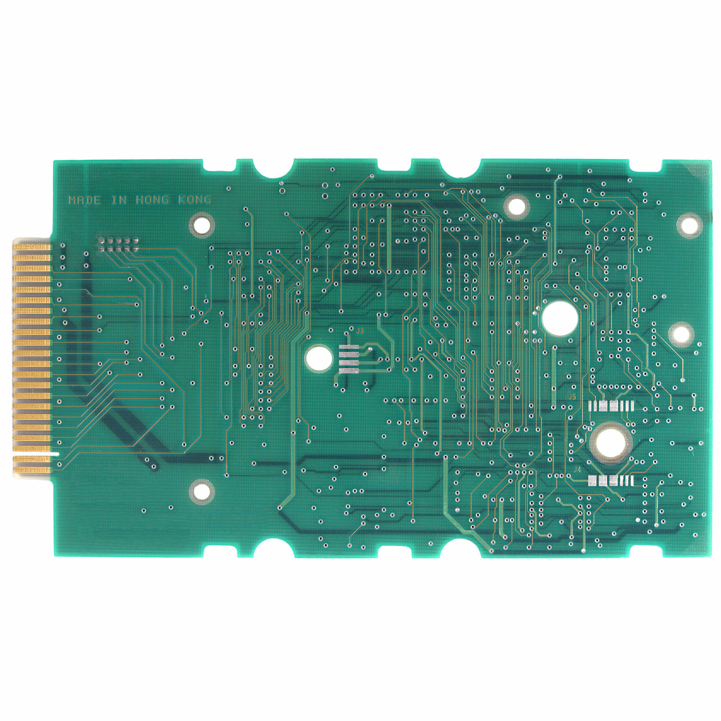
Backdrill in PCBs removes stubs in vias to improve signal integrity and impedance control, crucial for high-frequency, multilayer boards. It’s vital in communication, servers, medical, and aerospace applications.
2024/08/01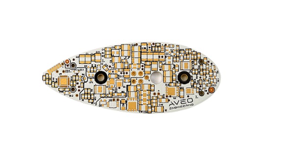
Aluminum PCBs are widely used electronic boards with comparatively better heat dissipation properties. The aluminum core cools down the components of the product, thereby improving its performance. These are eco-friendly, light, and strong PCBs and hence appropriate to be used in audio equipment, power supplies, and lighting products such as LED lighting.
2024/07/24