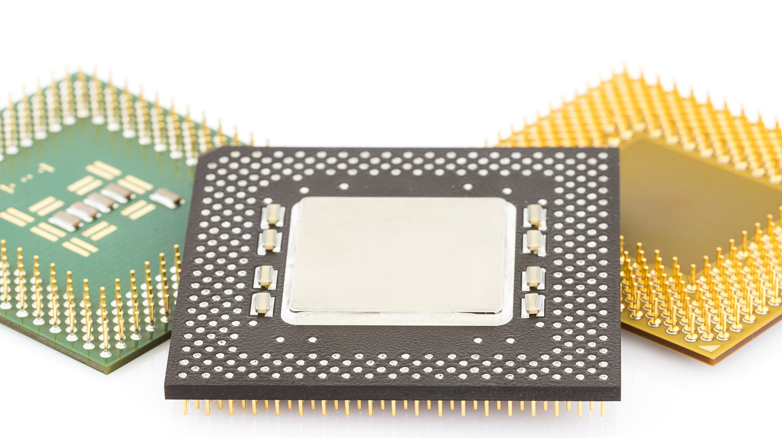
LGA vs. PGA vs. BGA
LGA, PGA, and BGA are IC packaging types critical for device design. LGA is compact; PGA allows easy upgrades; BGA is for high-performance needs.
Integrated circuits have also significantly evolved from the large ICs of the 1990s to small, yet powerful chips that are used to date in modern technologies. Such development has been possible through making small, efficient computing devices. Key to all such evolution are mainly three IC packaging types: Land Grid Array, Pin Grid Array, and Ball Grid Array. Each of these packages has different characteristics and usages, and thus greatly affects the electronic device design and functionality. The following article will explain the features of LGA, PGA, and BGA packages, outline the advantages and challenges that each faces in the electronics industry, and describe typical applications.
Ball Grid Array (BGA)
BGA is a surface mount package technology, normally utilized for integrated circuits. The high-density connections are provided through a grid of solder balls that are on the bottom side of the IC in rows and columns. This design maximizes the number of interconnections possible, making it suitable for complex and high-performance devices.
Advantages
Efficiency in Space: BGA packages are compact, taking up less space on the PCB, thereby enabling manufacturers to create small-sized devices without having to sacrifice much performance.
Improved Heat Dissipation: The grid of solder balls aids in good heat distribution and dissipation, therefore reducing the chances of overheating.
Low Electrical Impedance: The short and straight path for the connections allows low impedance for better signal speed and reliability.
Reworkability: BGA packages allow for deballing and reballing, hence, the replacement of old solder balls that can extend the lifecycle of the device.
Portability and Flexibility: The BGA chips are easily portable between devices as their solid design ensures that they deliver consistent functionality.
Challenges
Difficulty in Inspection and Repair: Owing to the fact that solder connections are under the chip, X-ray imaging is generally required to inspect them, and repairs require special skills and equipment.
Complex Soldering Requirements: Soldering BGA packages requires precision, and hence, the equipment is more complex, which introduces challenges in the soldering process.
Application Limitations: Most BGA packages are utilized with multi-layer circuit boards. This confines the uses of BGAs to only devices that support the use of such complexity.
Applications
BGA packages find profound applications in high-end computers, CPUs of personal computers, servers, and networking equipment-all those places where space, heat management, and electrical efficiency are of essence.
Pin Grid Array (PGA)
Pin Grid Array: The PGA is a method of packaging in which there is an array of pins projecting from the bottom of the IC, designed to fit into corresponding holes on the PCB. This provides a very good mechanical and electrical connection, especially in devices that require modularity and ease of upgradeability.
Advantages
Ease of Maintenance and Replacement: The design with a pin-in-hole feature enables the removal and replacement of chips without desoldering, which further reduces the complexity in maintenance.
Reliable Mechanical Connections: Physical insertion of pins into sockets provides a stable mechanical hold, reducing the risk of disconnections during operation.
Wide Legacy Support: Established prevalence of PGA over decades enables compatibility with most of the existing systems and sockets.
Limitations
Pin Fragility: The pins can be damaged by bending or breakage during handling and installation, requiring careful manipulation.
Limited Connection Density: Compared to BGA, the number of connections is limited, which can restrict miniaturization and higher integration density.
PGA Variants
Ceramic Pin Grid Array (CPGA): Uses ceramic as the base material, known for excellent thermal conductivity, used in older processors.
Plastic Pin Grid Array (PPGA): Uses plastic as the substrate. Plastic provides cost-effectiveness and fair thermal performance. This package form factor is standard among Celeron processors.
Staggered Pin Grid Array (SPGA): Has staggered pins to provide higher pin counts. Can be utilized by most new processors with over 200 pins.
Flip Chip Pin Grid Array (FCPGA): The ICs in this package are mounted face-down, thereby increasing its electrical performance and heat dissipation.
Applications
PGA finds the most applications in desktop CPUs like those manufactured by AMD. It plays a key role in any computing environment that requires the ease of upgrading and replacing components.
Land Grid Array (LGA)
Land Grid Array (LGA) is another form of IC packaging, where the electrical contacts are as flat pads or lands on the bottom side of the chip. The contacts align with matching pads on the PCB for a secure connection through a socket mechanism.
Advantages
Compact and Efficient Design: LGA packages have more compact space to accommodate a higher number of contact arrays, saving space on PCBs.
In-Reliability in Connections: The design minimizes the risk of pin damage since the contacts are on the circuitry rather than protruding from it.
High Electrical Performance: Low inductance and capacitance due to lead length minimization allows for high-frequency applications.
Challenges
Complicated Mechanisms in Sockets: The use of LGAs involves precise and sometimes very complicated socket designs, which can complicate the process of assembly.
Repair Issues: This is less easy to repair or change pins on the board as compared to PGA.
Applications
The LGA package has come into great use within high-performance processors from different vendors, including Intel, for instance, on servers and high-end desktops, where efficient usage of space and electrical performance become important.
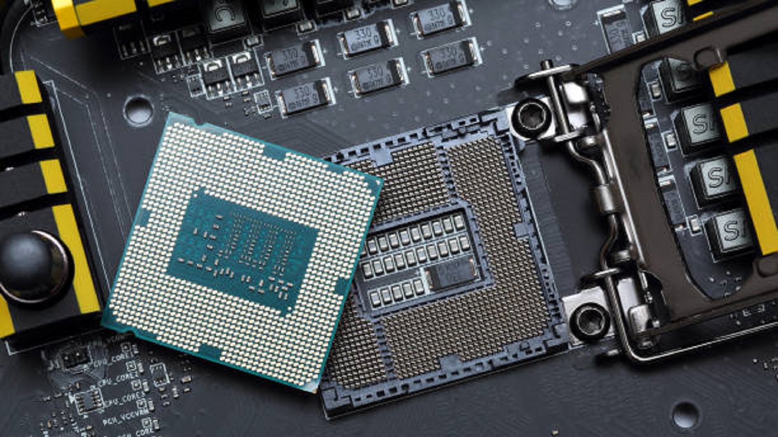
Selection among LGA, PGA, and BGA packagings strongly depends on application-specific requirements, including issues of space constraints, thermal management, electrical performance, and the complexity of the system design.
LGA dominates in high-performance, compact applications that need to have strong and rugged connections without the risk of pin damage. PGA excels in applications that require easy upgradeability and replacement, as is commonly the case in desktop computing environments. BGA realizes great importance in advanced electronics, where saving space is of essence and electrical performance is paramount. This encompasses consumer electronics such as smartphones and laptops.
The same understanding of these distinctions enables the engineer and designer to optimize performance and reliability in devices for ultimate innovation and efficiency in modern technology solutions. Each IC packaging type addresses specific needs, and its continued evolution and application form the base for the support of advancements across the electronics industry.
Hot Tags:
Contact us

If you can't find what you're looking for, please contact us.
Article
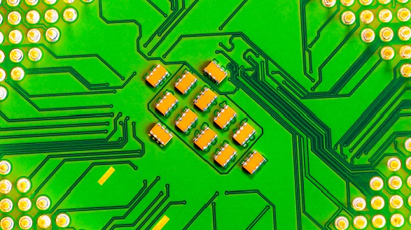
The article compares Ball Grid Array (BGA) and Land Grid Array (LGA) packaging technologies for mounting microprocessors on PCBs. It details their pros and cons, applications, and factors to consider for optimal design choices.
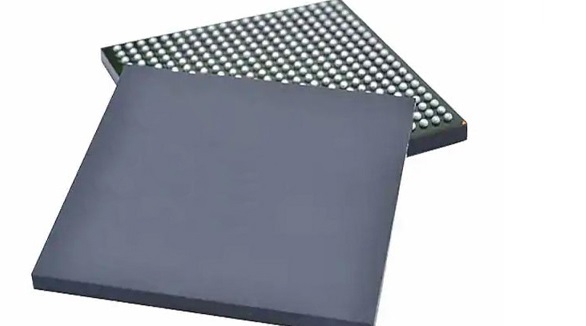
Compared to THT, SMT offers better miniaturization and weight reduction in any electronic application. With the use of BGA packages, high-assembly density, reliability, and improved performance are achieved; on the other hand, this requires a rework and inspection that is not really common. PCBX specializes in the area of advanced SMT and BGA assembly to help drive modern requirements of compact electronic devices.
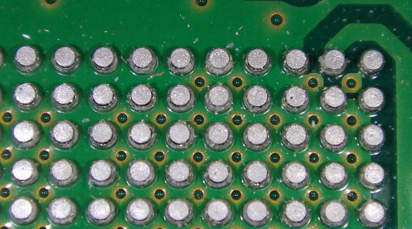
In the late 1980s, when electronics began to shrink, BGA packaging was developed to integrate more connections within a given area. Today, BGA is widely used with high-connection chips—processors being a good example. BGA uses solder balls at the bottom of the chip to connect it to the circuit board. It provides high density along with good heat dissipation and fast signal transmission, one of the main reasons it is ideal for modern electronics. However, it requires precise techniques of soldering in BGA manufacturing.

