Main PCB
The main PCB is crucial for mounting and connecting electronic components, vital for device performance. It supports design and manufacturing innovations.
Within the modern context of a digital world, the main PCB is the most critical element that ensures the perfect functionality of electronic devices. At the heart of everything-from smartphones to industrial machinery-the main PCB acts as the physical and electrical foundation for mounting all the required components. Knowledge of its design, components, and manufacturing would therefore be core to anyone with interests in electronic device performance. This article takes a close look at the details of the main PCB and its significance in the field of electronics.
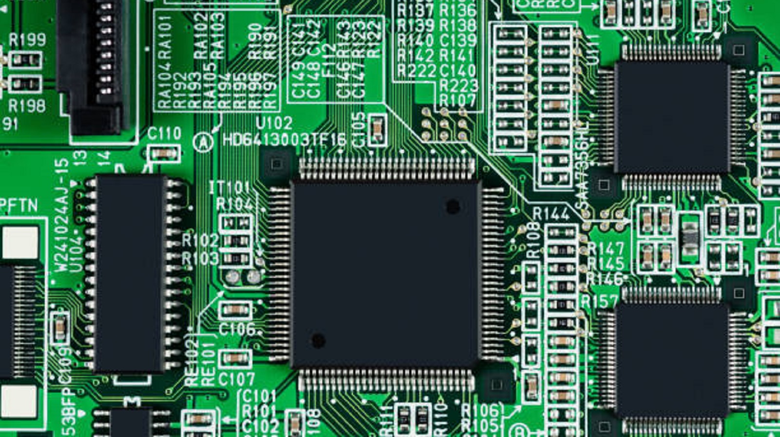
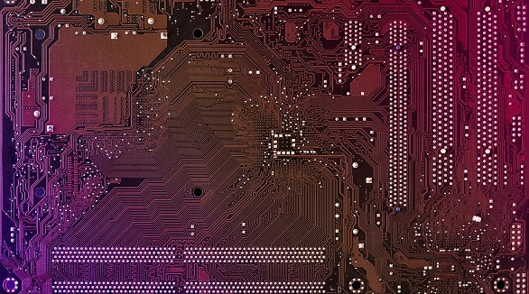
A main PCB is a flat board designed to offer mechanical support with the ability to provide electrical connections using conductive paths, pads, and traces. This board is used for two purposes: it securely mounts components in their correct locations and establishes reliable electrical connections between those components.
The main PCBs range from single to multilayered in design, depending on their field of application and degree of complexity in connectivity. Multilayer PCBs allow for advanced routing and provide better signal integrity, yet are more expensive and take much longer to make.

Key Components of a Main PCB
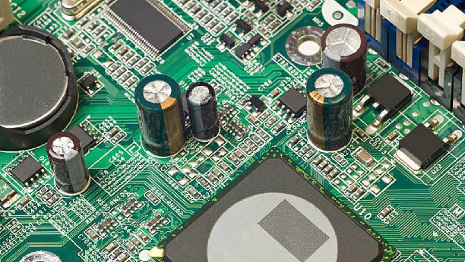
The main PCB hosts different components, which all have some vital functions in the running of the device:
Capacitors: These devices store and release electrical energy to stabilize voltage and fluctuations of power in the circuit.
Resistors: These control the flow of current, creating voltage drops while dissipating energy in forms of heat. Resistors are identified by a color-coded system that shows their values of resistance.
Sensors: These detect changes in environmental variables and convert them into electrical signals that may be processed further by other components in a circuit.
Diodes: One-way current passes while barred in the opposite direction, providing reverse polarity protection to several circuits. The common diode used for indication is a Light Emitting Diode (LED).
Inductor: Stores energy in a magnetic field, normally utilized to filter out signals and prevent high-frequency interference.
Transistors: Either amplifiers or switches which control electronic signals on a PCB. The most usable type of transistor is a bipolar transistor consisting of collector, emitter, and base.
Materials Used for Main PCBs
Materials used in main PCBs influence the performance and reliability of boards:
Substrates: The base material could be rigid, such as FR4, or flexible, which includes high-temperature polyimide films. It depends on the type of application.
Copper Layer: This layer is used to conduct electrical current through the board.
Solder Mask: It is a protective coating that prevents the copper layers from oxidation and avoids accidental short circuits during soldering.
Silkscreen: It labels components and denotes settings; thus, it provides the essential guide points directly onto the surface of a PCB.
Design Considerations for Main PCBs
A well-designed main PCB ensures high performance and long-term reliability. Key considerations include:
Signal Integrity
Effective trace routing and impedance matching are important to ensure signal integrity, no delay, and proper data transfer.
Thermal Management
Components generate heat, and in compact spaces, the use of heat sinks, thermal pads, and adequate ventilation becomes essential to maintain functionality and prolong component life.
Power Distribution
Proper power distribution minimizes voltage drops and electromagnetic interference, ensuring stable operation across the board. Strategic routing and component placement are essential for an efficient power network.
Component Placement
Optimal placement reduces trace lengths and minimizes parasitic effects, enhancing the board’s performance. This careful layout helps in minimizing interference and maximizing efficiency.
Layer Stack-Up
For multilayer PCBs, a well-designed layer stack-up separating power, ground, and signal lines reduces potential interference, boosting overall functionality.
Main PCB Fabrication Process
A main PCB fabrication entails the following steps with quality and functionality in mind :
Imaging the Circuit Design: The process involves a photo tooling or direct imaging to outline the circuit layout.
Copper Etching: Removal of excess copper to outline circuits and pads on the board.
Lamination: Layer lamination under pressure and heat to form a cohesive PCB structure.
Drilling: Creating holes for vias and component leads to establish electrical connections and allow component mounting.
Solder Mask Application: Coating the board to protect against oxidation and facilitate soldering.
Surface Finishing: Applying finishes like HASL or ENIG to enhance solderability and prevent corrosion.
Inspection and Testing: Comprehensive quality checks to verify the PCB meets design and performance standards.
Challenges in Main PCB Development
Developing a reliable main PCB entails overcoming several challenges:
Component Miniaturization: Smaller components require precision soldering and placement.
Heat Management: Powerful components require effective methods of heat dissipation.
Signal Interference: With higher frequencies, better shielding and trace design become required to reduce interference.

As technology evolves, so will the capabilities and configurations of main PCBs. The main PCB will continue to evolve with innovations in flexible PCBs, enhanced materials, and sophisticated design techniques, driving the development of more efficient and compact electronic devices.
Serving as the central part of an electronic device, the main PCB is crucial in integrating several electronic components into one workable system. By following best design practices and introducing state-of-the-art manufacturing methods, manufacturers are able to provide high-performance and reliable PCBs that will be indispensable for today's increasingly complicated technologies. At PCBX, we continue to drive innovation and excellence in PCB design and manufacturing, ensuring every device operates at its optimal potential, now and in the future.
Hot Tags:
Contact us

If you can't find what you're looking for, please contact us.
Article

Populated circuit boards integrate electronic components for efficiency and reliability, utilizing SMT and THT for diverse applications across industries.

Breadboards and protoboards are key prototyping tools in electronics. Breadboards allow for flexible, solderless circuit design, while protoboards provide durable, soldered connections for finalized designs.

Understanding core and prepreg materials is crucial for PCB performance and manufacturability. Core provides stability and dielectric properties, while prepreg binds layers. Both affect signal integrity, mechanical stability, and thermal performance.