- Products & Capabilities

- Simulation Design & EDA

- About
- Resources
Mastering PCB Printing: Processes and Benefits


PCB printing services are crucial for transforming complex designs into efficient parts, offering precision, cost savings, and access to advanced technologies.
In the 21st century, this importance has grown exponentially from smartphones and laptops to complex industrial systems. Due to the increase in demand by global consumers for smaller and powerful electronic devices, the role of PCB printing services is becoming increasingly important. These services have been acting very importantly in converting complex designs into tangible and efficient technological parts. The article examines the complex processes defining PCB manufacturing, elucidates the spectrum of services carried out by the manufacturers, and discusses the various benefits derivable from leveraging professionals in this key industry.
The Role of PCBs in Modern Electronics
PCBs play a major role in connecting various electronic components for smooth running operations on a device. These attributes of compactness, versatility, and reliability have turned them into an indispensable part of electronic manufacturing-from light to high-tech production companies. The manufacture of PCBs faces several technical challenges that must be addressed in production, including impedance control, optimization of copper weight, and accurate multilayer alignment. Many companies thereby rely on special PCB printing services that are fully equipped to produce such intricacies in electronics designs with expertise in technology and experience. In summary, this explains why there exists a dependence by many companies upon specialized PCB printing services which an expert, by the use of technology with lots of experience.
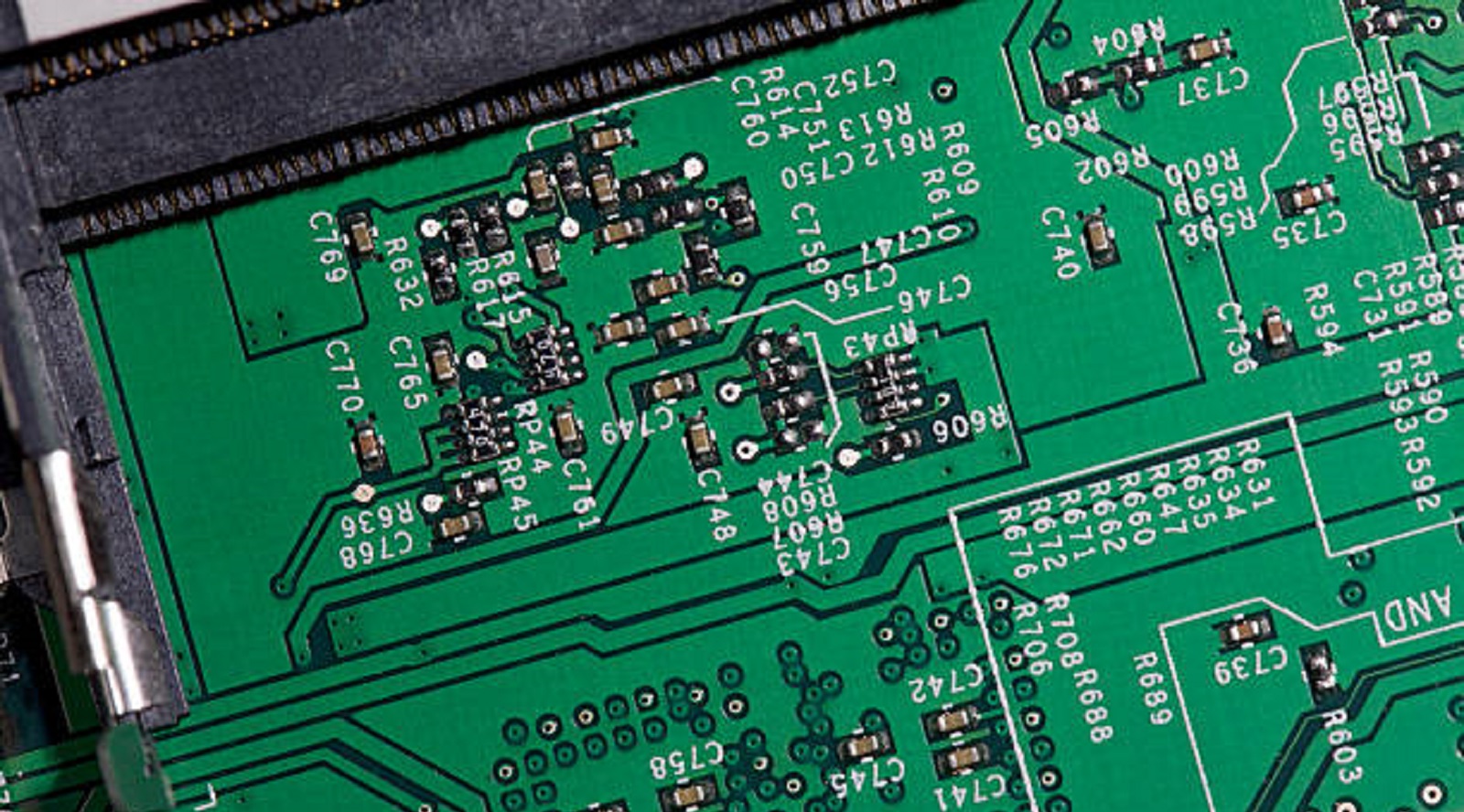
Creation of Design and Gerber Files: The design engineers create a schematic design using any CAD, like Altium Designer or Eagle. Later, this design is converted into Gerber files. These are basically the blueprint that contains all the details about every layer in the PCB. It accurately defines the size, location, and configuration of every copper trace, pad, and via to make sure the manufacturer replicates the design correctly.
Material Selection and Fabrication: After the Gerber files are delivered, manufacturers make use of an appropriate base material, which usually consists of FR-4, since it is inexpensive and resistant. In applications that need high frequency or specialty, Rogers or polyimide-based materials are chosen. In fabrication, the copper substrate with cladding is etched based on the design given in the Gerber file. When a PCB has multiple layers, these are aligned and bonded very accurately, which again requires high precision to prevent any functionality issues.
Drilling and Metallization: Holes required for component leads and vias are drilled with the use of highly specific machinery. Then, these holes are metallized to ensure the best electrical connection, so important for both the integrity and functionality of the PCB.
Solder Mask Application: This is a protecting layer, normally green in color, applied over the copper traces of the PCB to avoid short circuits and environmental damage. In this stage, preparation for the next steps in component soldering and board assembly is also done.
Surface Finishing: The exposed copper areas are finished with a surface finish (ENIG: Electroless Nickel Immersion Gold, HASL: Hot Air Solder Leveling among others) to improve solderability and prevent corrosion. Finishing may affect performance and the life span of a PCB.
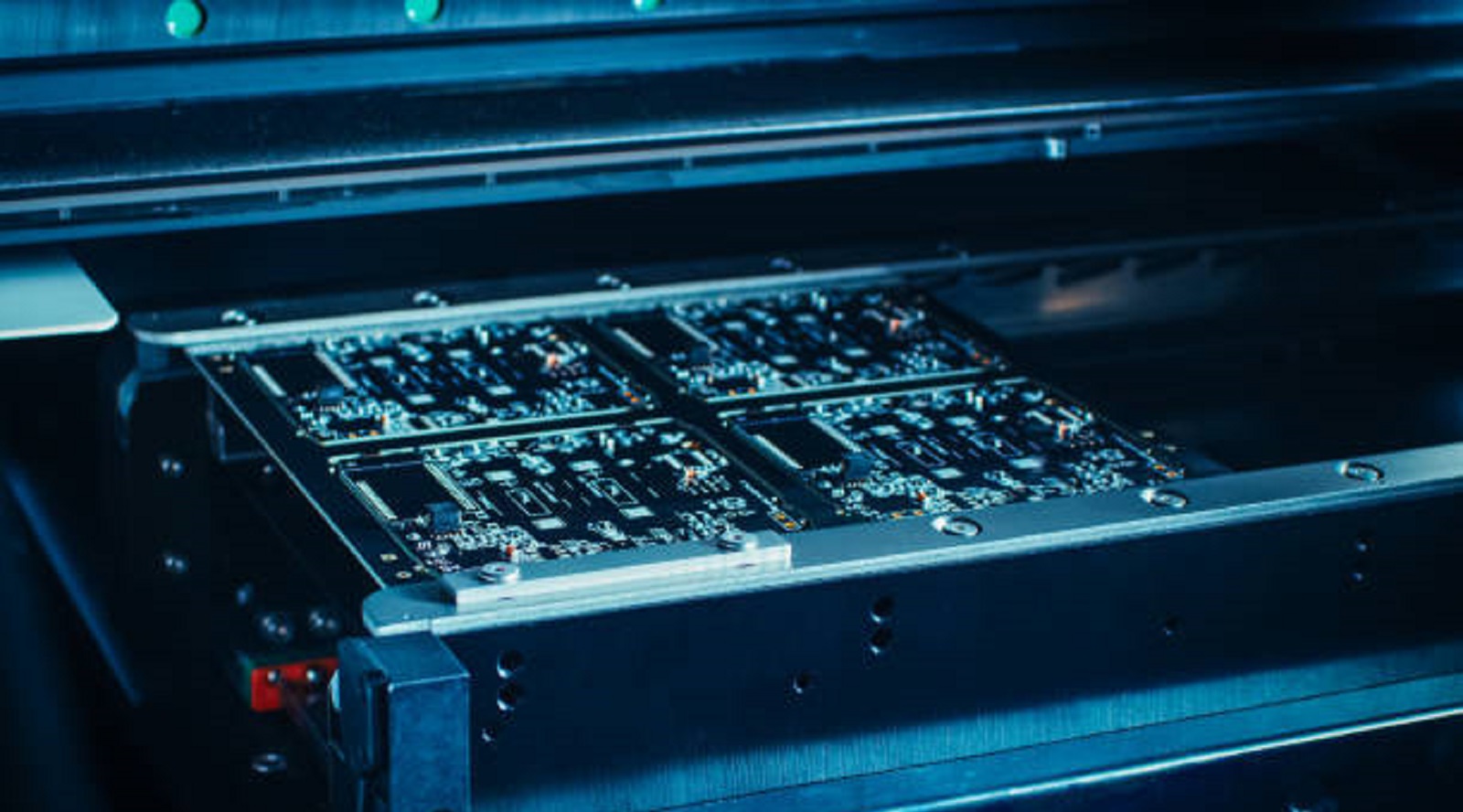
Component Assembly and Testing: According to design specifications, SMT or THT mounts and solders components to the PCB. After assembly, the board undergoes rigorous testing to ensure that every function works to the specification and quality expectations of the design.
Various Services Provided by PCB Fabrication
PCB fabrication is done to meet a variety of client requirements. Some of the services it offers include:
Prototyping and Low-Volume Production: This service is important to test and validate PCB designs before scaling up to full production. Manufacturers offer rapid prototyping to produce small quantities that allow designers to evaluate performance and make necessary adjustments.
Mass Production: Once a design has been vetted and finalized, PCB manufacturers provide mass production services, offering economies of scale and optimized manufacturing processes to reduce costs per unit.
Specialized PCBs: Advanced applications in industries such as aerospace or medical normally use multilayer, HDI, or flexible PCBs. Such a service demands very sophisticated manufacturing with closer attention to quality since each has different requirements to meet strict standards for those respective industries.
Custom Surface Treatments: Application-specific requirements by customers extend to offering variations in surface treatments to enhance solderability and durability, including immersion silver and organic solderability preservatives.
Turnkey Solutions: Some manufacturers extend services from design assistance to final assembly and, therefore, make it much easier for customers to get into production while their products get to market faster.
Advantages of Professional PCB Printing Services
Availing professional manufacturers for PCB services come with a set of advantages, especially for those companies who would like to assure quality and efficiency:
Precision and Quality Assurance: These professionals give unprecedented attention to details in giving out high-quality boards with accurate specifications. Knowledge helps to eliminate or at the least minimize possible design errors, thus preventing any failure of your products.
Cost-Effective with Time-Savings: Outsourcing will reduce cost considerably and bring speed to your time-to-market. A professional PCB manufacturing service will have more significant resources that could facilitate them in availing economies of large scale and, accordingly, result in faster turnover times without any loss of quality.
Access to Advanced Technologies: Involvement of experienced manufacturers in PCBs opens a company's exposure to high-class processes and emerging technologies. This would be one important benefit when it comes to innovating products reliant on complex or high-performance PCBs.
Full-scale Testing for Compliance: It would also involve professional testing that guarantees the products' quality and safety standards internationally. It reduces defects and improves the reliability of products.
In the modern world of technology, PCBs are a core factor that drives innovation and functionality in electronics. The expertise of professional PCB printing services is needed in their creation due to the complex processes involved. Such services help companies transform complex electronic designs into reliable products, right from initial design through prototype testing to mass production. A business that leverages such capability and advances in technology from expert manufacturers can focus on innovation, ensuring that it delivers high-quality electronic devices to an ever-evolving market. From consumer electronics to highly advanced industrial technology, professional PCB printing services play an important part in such success.
Hot Tags:

Contact us

If you can't find what you're looking for, please contact us.
Article
In the fast-evolving electronics field, PCB performance hinges on dielectric material selection, crucial for signal integrity, thermal management, and reliability.
 2025/01/08
PCB libraries streamline PCB design with schematic symbols, footprints, and 3D models, boosting reliability and efficiency through effective management.
2024/11/15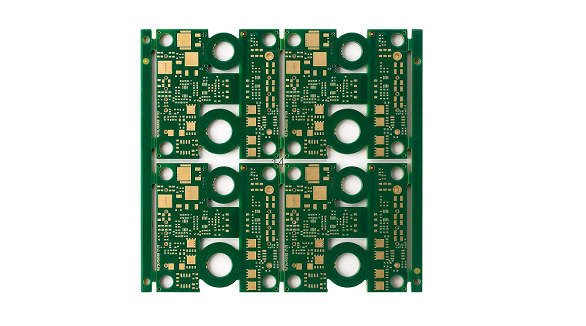
Most electronic circuits are mounted on PCBs, or Printed Circuit Boards, which provide mechanical support and electrical interconnection of electronic components. There are, however, special applications that involve the use of single and double-sided PCBs, multi-layer PCBs, or even rigid and flexible PCBs with aluminum backing, targeting medical, industrial, auto, and aerospace industries. They may use materials such as fiberglass, epoxy, aluminum, and others.
2024/07/25