- Products & Capabilities

- About
- Resources
Multilayer PCB Benefits and Applications


Multilayer PCBs, essential for advanced electronics, offer compact size, lightweight, and high performance, making them ideal for various applications despite higher costs and complexity.
PCB (Printed circuit board) is at the heart of most electronic devices today, with its basic operation determined by a complex interplay of components and wiring methods. Traditionally, PCB was fairly simple, constrained by the processing techniques available at the time. As technology has advanced, PCB has become increasingly sophisticated. The present landscape includes a plethora of innovative PCBs at work, ranging from flexible alternatives to ones that appear oddly formed. Multilayered PCBs are the most popular of these.
Multilayer PCBs are found in every sophisticated electronic device. The simplest of electronics, with not too many functions, use a single-layer PCB, while more advanced electronics, like motherboards of computers, have multiple layers. These multilayer PCBs have become frequent since modern technology has increased in complexity, while at the same time, advancements in manufacturing make these PCBs very small in size.
In this article, we will look into multilayer PCBs: what they are and what kind of applications, along with advantages, they render across modern electronics.
What is Multilayer PCB?
A multilayer PCB consists of three or more layers of conductive copper foil, with several double-sided circuit boards that are laminated and bonded together, having layers of heat-protective insulation in between. The outside layers confront the environment, while the interior layers link through vias similar to plated through holes, blind vias, and buried vias. Highly complicated PCBs of varying sizes can be manufactured inside this structure.
The invention of multilayer PCBs was necessitated by the need for better electronic functions. Noise, stray capacitance, and crosstalk have always been challenges to simple PCBs and, at the same time, demanding an advanced version for improved performance—hence, the multilayer PCB.
The multilayer PCBs are thin powerhouses containing double-layer PCB functionality inline space, in different sizes and thicknesses depending on the application, often ranging from four to twelve layers. Most designs contain an even number of layers to ensure that worries associated with such designs as warping are reduced and they remain pocket-friendly. Four to eight-layer applications are very common, while a device like a smartphone may come with about twelve layers. There are experienced manufacturers capable of producing multilayer PCBs that span nearly 100 layers, though this is an unusual configuration and very costly.
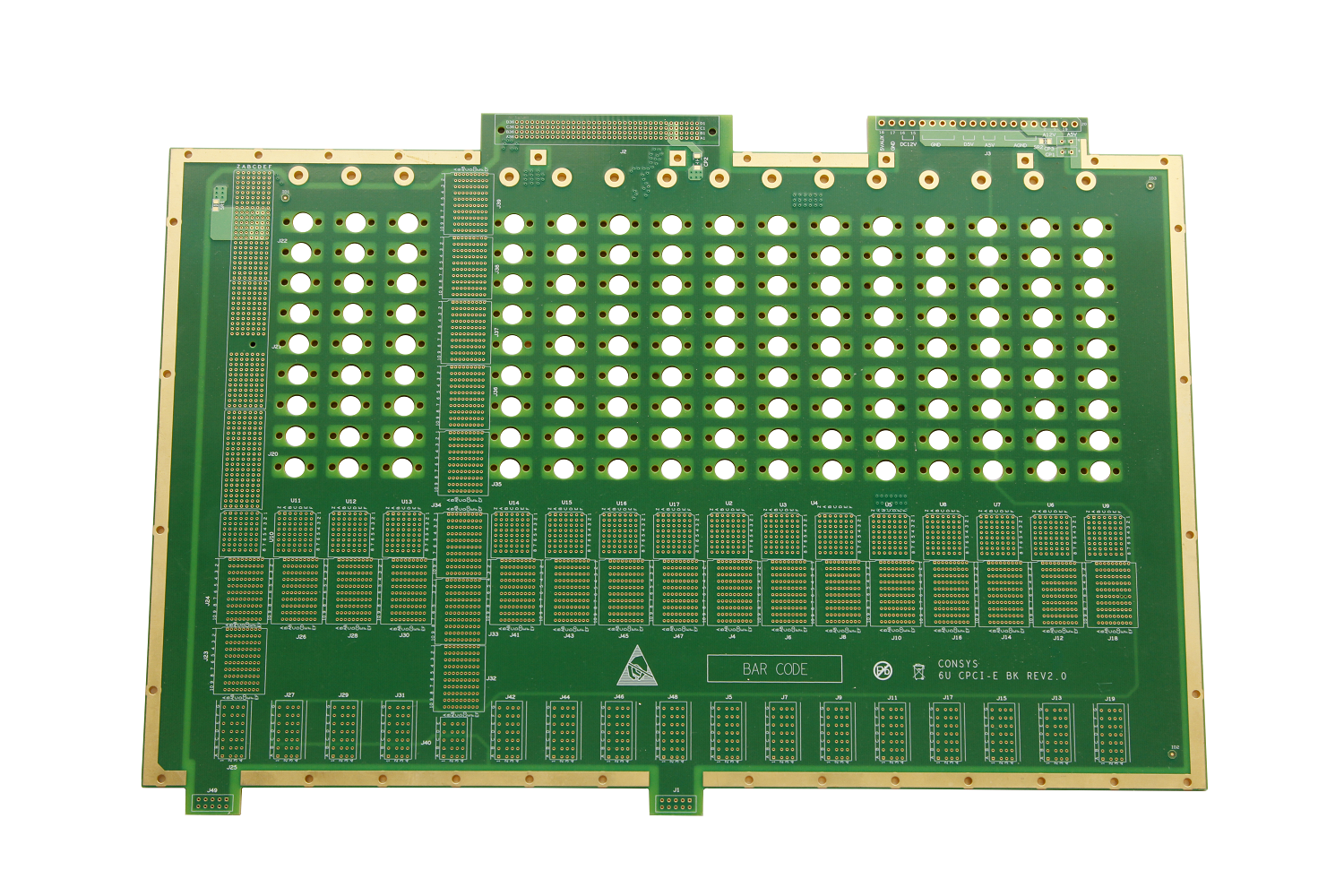 20-layer PCB
Despite the harder and more time-consuming labor, production, and relatively higher cost related to their activity, multilayer PCBs are at the core of most contemporary technology because of the many advantages it has over single and double-layer types.
Advantages of Multilayer PCBs
Technically speaking, multilayer PCBs have many design advantages:
- Compact Size: Multilayer PCBs are, by default, much smaller than other PCBs with comparative functionalities, which is quite beneficial for modern electronics, which look towards compact, yet powerful, devices such as smartphones, laptops, tabs, and wearables.
- Lightweight Structure: Avoiding the use of multiple connectors that are normally applied in single and double-layer PCBs further lightens the weight that multilayer designs offer support for in regards to modern electronics emphasizing mobility.
- High-Quality: The amount of work and planning that goes into their production usually results in better quality and reliability than their single- and double-layer counterparts.
- Improved Durability: Multilayer PCBs are designed with strong boards, capable of supporting the weight, heat, and pressure involved in their manufacturing process, making use of multiple insulation layers, which improves their overall durability.
- Greater Flexibility: Some multilayer PCB construction techniques are preferred where mild bending and flexing are encountered in the application; however, the addition of more layers can reduce this flexibility.
- More Powerful: These high-density assemblies provide both better connectivity and higher electrical performance in a small space area.
- Single Connection Point: Being designed as one piece, multilayer PCBs require only one connection point, which simplifies the design of most electronic products and aids in their reduction of size and weight.
- These features have made multilayer PCBs very valuable in mobile devices and high-function electronics, thereby setting their adoption between different industries.
Disadvantages of Multilayer PCBs
Despite many advantages, some disadvantages make multilayer PCBs less fit for use in some applications:
- Higher Cost: The intricacies of the design and manufacturing procedures, along with expensive equipment and labor-intensive work, make multilayer PCBs rather pricey than other single and double-layer ones.
- Difficult Production: The sophistication in design and the manufacturing process makes it more difficult to produce, where even a small defect in the finished product can render a PCB useless.
- Lower Availability: Not every manufacturer owns available machinery or technology; hence, multilayer PCB production is not as widely available.
- Experienced Designer Needed: Multilayer PCBs require experienced designers to avoid issues such as crosstalk and impedance because a small mistake in design may cause the generation of a non-functional board.
- Production Time: The added complexity prolongs the production time, in this way, it may impact the turn-over rate and probably delay the delivery time of products to customers.
- Despite these shortcomings, the usage of multilayer PCBs can strategically warrant their costs since they offer profound improvements over single-layer options.
Benefits of Multilayer PCB Over Single Layer PCB
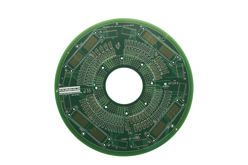 20-layer PCB
Compared with the single-layer PCB, multilayer PCB has improved in the following aspects:
- Assembly Density: Layering increases density; hence, it increases functionality, capacity, and speed.
- Smaller in Size: With multilayer designs, surface areas are achieved by the number of layers rather than size increases, thus enabling high-capacity PCBs for smaller devices.
- Lighter Weight: Fewer components means lighter weights for electronic solutions.
- Enhanced Structured Design Capability: Incorporating controlled impedance features, greater EMI shielding, and increased overall design quality allows multilayer PCB to perform better even with their compact size.
Multilayer PCB Applications
The demand for compact, workable electronic solutions makes multilayer PCB fit for a wide array of usages in fields such as:
- Consumer Electronics: From smartphones to microwaves, the trend toward multifunction smart devices drives the usage of multilayer PCBs.
- Computer Devices: Space-saving with high-performance feature of multilayer PCBs make it suitable for servers and motherboards, all in this genre.
- Telecommunications: Durability and functionality make multilayer PCBs fit for signal transmission, GPS, and satellite applications.
- Industrial: The strength and efficiency of multilayer PCBs adapt them to industrial controls and machinery.
- Medical Equipment: The compact, lightweight, and other functional characteristics make multilayer PCB suitable for the healthcare technology.
- Military and Defense: For high-speed circuits and compact designs, the low weight and durability of these boards are highly valued.
- Automotive: Increasing usage in the electronic systems that are used for control in vehicles.
- Aerospace: Multilayer PCBs are highly reliable, withstanding atmospheric stresses, so they find major usage in these fields.
Why Are Multilayer PCBs So Widely Used?
While directly raising costs and complexities, the trend towards miniaturization and multifunctionality in electronics prefers multilayer PCBs as the solution. With advancing technology, the decreasing cost of producing these PCBs will make them accessible to most diverged applications.
Multilayer PCB Production and Assembly with PCBX
PCBX provides one-stop PCB manufacturing and assembly with high quality driven by IPC Class 3, RoHS, and ISO9001:2008. Rest confident that our experience allows us to handle all of your complicated multilayer PCB requirements from beginning to end.
Interested in knowing more about our capabilities or getting assistance from PCBX for your multilayer PCB project? Find more on our website, or feel free to contact us directly with detailed inquiries.
Hot Tags:
Contact us

If you can't find what you're looking for, please contact us.
 2024/07/25