PCB Backdrill
Backdrill in PCBs removes stubs in vias to improve signal integrity and impedance control, crucial for high-frequency, multilayer boards. It’s vital in communication, servers, medical, and aerospace applications.
What is Backdrill in PCBs?
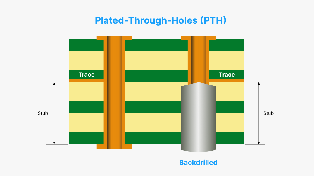
Backdrill is the process of removing the stub inside copper-plated vias in PCBs. Simply put, it is the part of a via that does not connect to any surface layer and typically serves no purpose. To understand what is meant by back drilling, consider a ten-layer board with a high-speed signal that needs to pass from the top layer to the bottom, as shown below. A via often spans all layers of the board, sometimes ranging from the eighth to the tenth layer, and has no function other than to form a pillar. This useless material can sometimes damage signal integrity and thus has to be drilled out from the backside. Back drilling became the term used to describe the process.
In multilayer PCBs, the use of unused vias or stubs can result in impedance mismatches in signal channels. The back drilling technique, in addition to blind and buried vias, is required to preserve signal integrity and performance for impedance-controlled high-frequency PCBs.
General Features of Backdrill
- Typical Usage: Used for boards with eight or more layers.
- Board Type: Most of the time, rigid boards.
- Drilling Specifications: The drilling diameter for the plated through-hole is less than the back drilling diameter by 0.2mm.
- Depth Tolerance: Tolerance maintained on the depth of back drilling is ±0.05mm.
Advantage of Backdrill
- Better Signal Integrity: Avoids unwanted reflection and cross-talk.
- Improved Impedance Control: It gives a greater degree of control of electrical characteristics.
- Lesser Crosstalk: The reduction of the interference of one signal with another de-couples vias in the board.
- Easy Fabrication: Reduces the dependence on blind and buried vias, making PCB fabrication easier.
Process Involved in Manufacturing of Back Drilling
- First Drilling: Use the PCB's positioning holes to attain first drilling with pinpoint accuracy.
- Filling of Positioning Holes: Fill the positioning holes with dry film to seal them and then plan the process of electroplating.
- Electroplating: The PCB is electroplated post-first drilling.
- Outer Layer Pattern: Develop the outer layer pattern.
- Pattern Plating: The positioning holes are resealed with dry film and the outer layer pattern is pattern plated.
- Back Drilling: The required plated holes are back drilled by utilizing the initial drilling positioning holes.
- Cleaning: The back drilled holes are cleaned thoroughly to ensure no residual debris is left in the holes.
The Back drilling Process
The main purpose of back drilling is to remove what is called unused portions of the plated through-holes, which have no connectivity, and the functions of transmission to avoid the siding potential such as signal reflection, signal scattering, and delay are important in high-speed signal transmission.
Various Application Areas of Back-drilled Boards
The back-drilled boards find its application area in the following:
- Communication Equipment: It is used to support high-frequency signal integrity.
- Large-Scale Servers: This is one of the known servers where data integrity and high-speed transmission matter.
- Medical Electronics: Ensuring reliable and precise functions in the electronics of a medical device.
- Military and Aerospace: For tough and high-performance circuit needs in many applications requiring toughness.
About PCBX
PCBX has never stopped serving the diversified global customers and their applications over various industries by providing a full range of PCB services, including PCB prototype and batch production, PCB assembly (SMT), electronics module sales, and CNC machining. We are always sure of the quality, on-time delivery, cost-effectiveness of our products, and ability to meet any special demands in electronics.
Hot Tags:
Contact us

If you can't find what you're looking for, please contact us.
Article

Annular rings are crucial for reliable PCB electrical connections. Proper sizing, understanding issues like tangency and breakout, and best practices ensure optimal performance and reliability in electronic circuits.
Vias—blind, buried, and through-hole—are essential in multi-layer PCBs, enabling signal and power transfer between layers. Covering techniques like tenting and plugging with solder masks enhance PCB reliability and performance, crucial for compact designs.
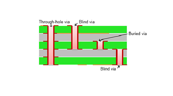
A printed circuit board includes a number of copper foil circuits, which are interlinked by vias. Via (through-hole, blind, buried, stacked, microvias) provides critical interlayer connections in high-density interconnection boards. Blind and buried vias increase the density of boards without adding size; hence, they are imperative for modern trends of miniaturization and high-speed signal transmission. These vias are plated with conductive materials, usually copper, so the electron flow can happen without much effort. Although advanced via types, like stacked vias, cost more, they save up much space and significantly improve routing capacity.
