PCB Bow and Twist
Addressing PCB bow and twist ensures reliability in advanced tech, focusing on intrinsic/extrinsic causes, refining design, and production for optimal performance.
In the ever-changing world of electronics, maintaining the mechanical robustness of a printed circuit board becomes the ultimate priority. With the increasing demand for smaller and technologically advanced electronic gadgets, ensuring the reliability and performance of printed circuit boards has become more critical than ever. Of all the mechanical deformations, bow and twist are two of the most prevalent problems the manufacturing concerns need to deal with and thus may highly affect functionality. The following article looks at these deformations, their causes, and the strategies available to fight them to further improve PCB performance and reliability.
What is PCB Bow and Twist?
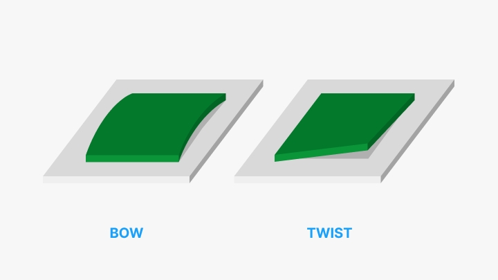
PCB Bow: Refers to the deformation that makes the PCB assume an arc either upwards or downwards along its length or width. For easier understanding, imagine a gentle hump in the middle of the board: such bowing can present challenges during assembly-misaligning components-and sometimes even jeopardizes device functionality and reliability.
PCB Twist: The PCB assumes a helical twist. For this condition, one corner of the PCB is out of alignment with the other three, as one wrings a handkerchief. This twisting increases mechanical stress on solder joints and components. Early failures in electronic assemblies often result from this and may be seen especially in systems exposed to some mechanical or thermal stress.
Modern Components Contributing to Bow and Twist
Unstoppable development of electronic components is constantly shifting the position of frontiers for PCB technology. The modern family of SMT components with their smaller and finer pitch footprints requires high-density interconnections, exact pattern accuracy, and excellent flatness. In turn, PCBs are often designed as SMT components in larger assemblies, contributing even more to the already strict demands of ideal flatness, forcing effective management of bow and twist both during and after the assembly process.
Causes of Bow and Twist
Bow and twist can be better avoided if their causes are known. For this reason, causes of bow and twist are divided into intrinsic and extrinsic:
Intrinsic bow and twist: The reason for the generation in making a PCB, particularly when lamination cure processes are involved. These deformations track back to manufacturing-related issues such as malfunction of the lamination press, cross-plying of prepreg or inner layers with misaligned warp and fill directions, and imbalanced or incorrect glass ply construction. Nonsymmetrical builds add to copper distribution that is not in balance, causing aggravation of these intrinsic deformations.
Extrinsic Bow and Twist: On the other hand, occur after lamination; these are typically correctable. These deformations have causes for external factors such as mechanical handling, heating in solder mask or legend curing, and hot air solder leveling, in addition to issues during PCB assembly.
How to Address Bow and Twist?
Along with the effect of bow and twist, effective battle requires that a full review of design and production processes be carried out by PCB manufacturers, which ought to focus on the following strategies.
Refine Lamination Process: Since lamination is a critical process in bonding the layers of the PCB together, it must be done carefully. Pressing cycles and temperature should be optimized to ensure better performance. Longer cycle times, with specific temperature settings and exactly applied pressure, enables resin in the prepreg to flow appropriately and form strong bonds between the layers.
Employment of Robust Prepreg and Symmetrical Inner Core Designs: Selection of prepreg itself is one of the key factors in bow and twist management. The right balance of customer specification and selection of materials that would provide better stability needs to be done by manufacturers. Ensuring symmetry in the build, although it may require recalibration of impedance, does a lot for enhancing PCB stability and flatness.
Symmetrical Copper Distribution: Uneven thermal and mechanical stresses are due to the unbalanced copper distribution. Symmetry of copper weight has to be maintained for all layers. The distribution within the layers themselves has to be in a state of balance. One may contemplate strategic copper filling with dummy pads or crosshatched copper to avoid low-pressure areas.
Areas of Low Pressure: Designs with high layer count often have tendencies toward areas of low pressure, which enhance these deformations. These can be remedied by the implementation of copper filling strategies in order to maintain the same pressure within the PCB.
Split Ground Plane and Breakaway Area Management: Split planes acting like bend indicator lines in designs should be judiciously managed to avoid accentuating bow and twist. It is important that the breakaway areas mimic the copper distribution in the main PCB for flatness and structural integrity.
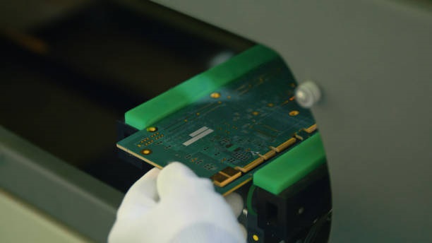
The understanding and management of intrinsic and extrinsic factors represent a very sophisticated approach toward bow and twist management in a PCB. This is further done by refinement in manufacturing processes, appropriate material selection, and optimization in design strategies, which help value addition in performance and reliability for the products of PCB manufacturers like PCBX. This proactively meets the stringent requirements of modern electronics while simultaneously taking the industry ahead to support innovation and technological advancement.
While the electronics industry is drifting towards greater complexity and density, vigilance by the manufacturer in managing such potential deformations due to bow and twist becomes very critical. Accordingly, provided there has been careful planning and exact execution, manufacturers are in a position to ensure that their PCBs demonstrate consistent and reliable performance to meet the ever-evolving demands of the electronics industry.
Hot Tags:
Contact us

If you can't find what you're looking for, please contact us.
Article
Plated-through slots (PTS) in PCBs are copper-plated apertures for electrical connectivity, offering space optimization, reduced soldering voids, and improved surface use.
Backdrill in PCBs removes stubs in vias to improve signal integrity and impedance control, crucial for high-frequency, multilayer boards. It’s vital in communication, servers, medical, and aerospace applications.
Conformal coating protects PCBs but sometimes needs removal. Local removal uses soldering, solvents, or mechanical abrasion. Full removal is more labor-intensive, involving chemical stripping or extensive mechanical abrasion.