- Products & Capabilities

- Simulation Design & EDA

- About
- Resources
PCB Encapsulation


PCB encapsulation offers vital protection against environmental, mechanical, and security threats, ensuring the reliability and longevity of modern electronic devices.
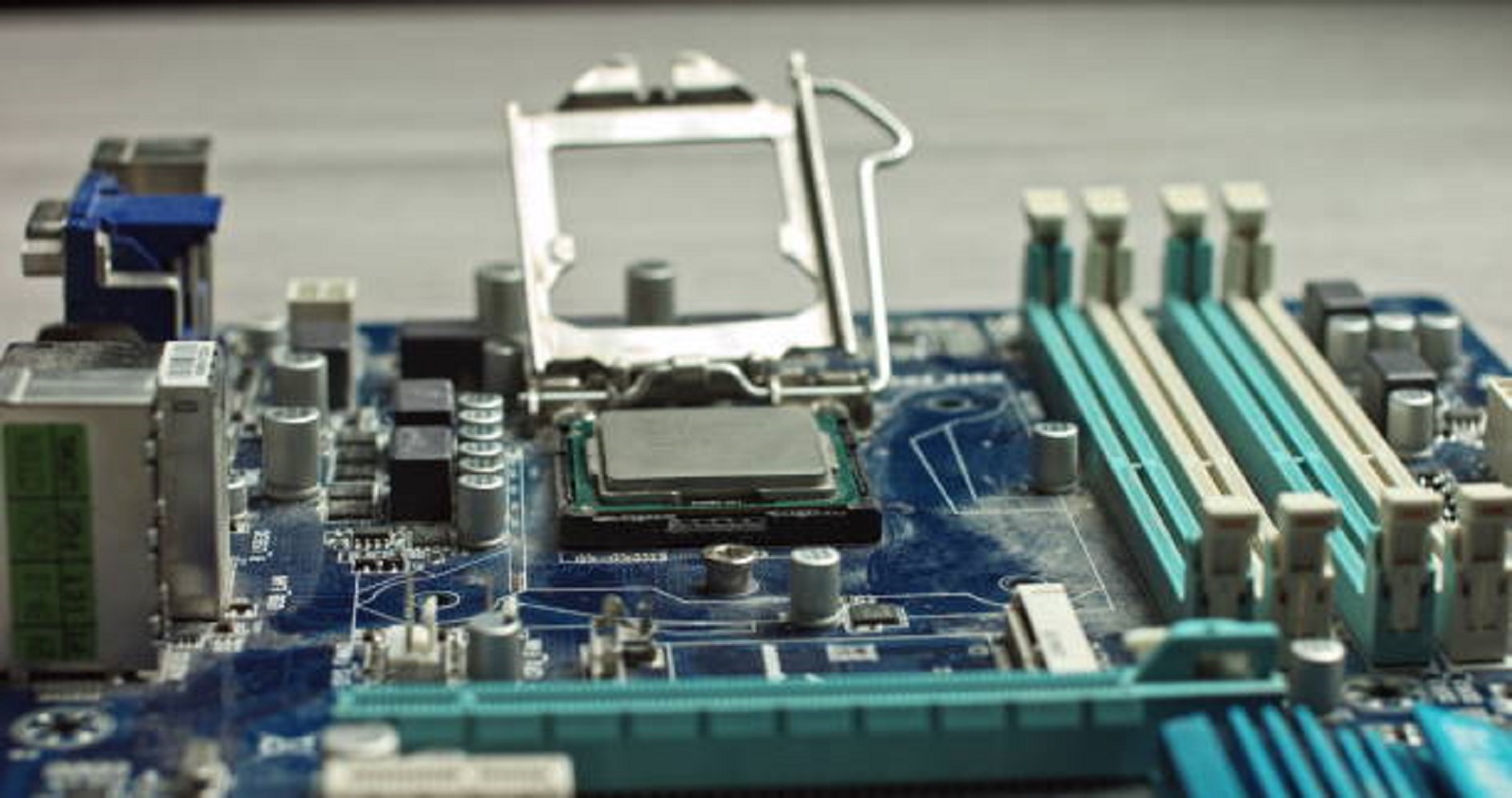
With the miniaturization of electronic devices while their complexity increases, high demands for assurance of their reliability and longevity should be addressed. At the center of such amazing technologies are Printed Circuit Boards-PCBs, whose protection against environmental and mechanical stress has to be robust. Encapsulation of Printed Circuit Boards crops up as one of the imperative processes in extending comprehensive protection to such electronic components. This article explains various aspects of the encapsulation process, its significance, and its applications in modern electronics. Sometimes known as potting, encapsulation is a method of completely covering an assembly in a thick layer of protective material. Unlike conformal coatings, which offer a thin film of protection, encapsulation gives a thicker layer of material. The process provides an excellent barrier against environmental factors such as moisture, dust, chemicals, and mechanical shock. The process of encapsulation shields the PCB from external damages, which also guards the PCB from unauthorized access and tampering as it obscures the PCB's components.
Why PCB Encapsulation is Important
Environment Protection: Encapsulation acts as a very strong barrier to the environmental elements, including moisture, dust, and corrosive chemicals that can destroy the functionalities of electronic gadgets. The protection is crucial to equipment serving under unfriendly operation conditions, including industries, power plants, and mines.
Mechanical and Thermal Reliability: The encapsulating material absorbs mechanical stresses and vibrations that may cause detachment or fracture of the components. Besides, encapsulants with thermal conductive properties help dissipate heat, thus preventing overheating and ensuring optimal performance of the device.
Security: Most encapsulating materials are opaque, adding to security by obscuring the layout of a PCB and components. This makes it difficult to reverse engineer and tamper with the circuitry, hence protecting intellectual property.
Electrical Insulation: Encapsulation offers better electrical insulation, which is required to avoid any sort of short and ensure safety, especially in high voltage applications.
Advantages and Disadvantages of Encapsulation
Advantages:
Provides protection against environmental contaminants and mechanical shock
Security due to obscurity of component view
Provide good insulation in high voltage
Help in damping vibration and reduces EMI/RFI interference
Disadvantages:
Encapsulation increases the device weight and might complicate the device handling.
More complicated and costly process compared to conformal coating.
Repairs and reworks involving encapsulated PCBs are tricky to deal with.
Encapsulation vs. Conformal Coating
Which method to use, between PCB encapsulation and conformal coating, depends on the application. The conditions that call for extreme measures are best handled by encapsulation, which offers robust, all-encompassing protection. Conformal coatings work well when weight, flexibility, and cost are critical, such as in consumer electronics. Both techniques have their specific advantages and should be selected according to the prevailing environmental conditions and functional demands that the electronics have to withstand.
Types of Materials Used in PCB Encapsulation
The type of encapsulation material is selected based on application needs. The common ones include:
Epoxy Resins: With very excellent mechanical strength and resistance to chemicals, especially in harsh environmental conditions, it protects robustly and finds many uses in applications that call for durability.
Silicone Gels: Being flexible, along with good thermal stability, finds their use in places that are exposed to temperature changes.
Polyurethane Resins: These are the resins that offer a balance between flexibility and hardness; thus, they are very effective in absorbing impacts and protecting against moisture.
Applications of PCB Encapsulation
Encapsulation finds applications in many fields:
Electronics and Electrical Components: It protects against environmental factors such as moisture and dust to maintain circuit integrity.
Photonics: This is used in LEDs, solar panels, and optical instruments to avoid interference from humidity and dust and to block harmful UV radiation.
Cables: Protects internal wires from moisture, chemicals, and sunlight, maintaining performance reliability.
Step-by-Step PCB Encapsulation Process
Following are some of the basic steps of the encapsulation process:
Placement: The PCB assembly is placed into an open pot or mold.
Pouring: A liquid potting compound is poured over the assembly until it's completely covered. This compound generally includes the addition of a hardener to help in its curing process.
Curing: The liquid sets to a shell that provides effective protection. The kind of compound applied—epoxy, silicone, or polyurethane—is based on the type of protection desired.
Challenges and Considerations
While encapsulation offers quite a few advantages, it also includes some challenges:
Heat Management: Encapsulation prevents natural heat dissipation and results in overheating unless thermally conductive materials are used.
Reparability: Encapsulated PCBs are practically impossible to repair, since accessing the components requires the removal or cutting of the encapsulant, which could easily damage the board.
Material Selection: The selection should be based on thermal, mechanical, and electrical requirements for appropriate application to best protect them.

PCB encapsulation serves a vital reliability and longevity interest for modern electronic devices by availing unequal environmental, mechanical, and security protection. In view of advances in technology, increasingly sophisticated encapsulation will be required; the type and method of application being carefully matched to the optimum in each specific case. Understanding how PCB encapsulation works will give companies a huge boost in leveraging this advantage and helping their respective technology products stay stronger, hence keeping ahead in the game through technological improvements.
Hot Tags:

Contact us

If you can't find what you're looking for, please contact us.
Article
In the fast-evolving electronics field, PCB performance hinges on dielectric material selection, crucial for signal integrity, thermal management, and reliability.
 2025/01/08
Button plating in flex PCBs enhances flexibility, reliability, and miniaturization, meeting modern design demands for smaller, highly functional devices.
2025/01/06
PCB edge mounting optimizes space, enhances modularity, and improves connectivity by placing connectors on board edges, aiding in flexible, efficient system design.
2024/12/11