- Products & Capabilities

- About
- Resources
PCB Etching: All You Need to Know


Etching is crucial in PCB production, removing unwanted copper to create conductive pathways. Techniques include chemical, laser, plasma, and photochemical etching, each with advantages and limitations ensuring PCB performance and reliability.
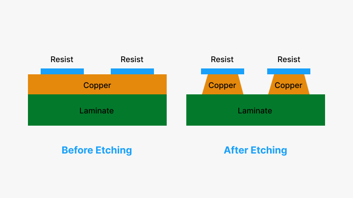
Etching is among the most basic steps for making a PCB. It consists of the selected removal of unwanted copper from the surface of the board so that only the conductive pathways, or traces, remain to interconnect the different electronic components. Quality of the resultant PCBs depends directly on the care and accuracy with which this operation is performed since it may affect the performance and reliability of the finished electronic product.
Traditional Techniques of Etching
Chemical Etching
Chemical etching is the most widespread method used in the production process for PCBs owing to its low cost and reliability. It is done by applying a chemical solution selectively to dissolve the unwanted copper.
Ferric Chloride Etching
Ferric chloride is a very corrosive chemical that efficiently reacts with copper. In the process, the required traces of the circuit are left intact, while the excess is dissolved away. This traditionally favored acid is effective and very cheap.
Ammonium Persulfate Etching
Ammonium persulfate is a substitute for ferric chloride that is much safer. It is nontoxic and gives high-quality results without giving away safety. Nowadays, this is a very common method since it is considered more eco-friendly.
In this process and the above traditional chemical processes, the board is masked with a resist material which prevents areas from the action of the chemical, so that only the exposed copper will be etched.
Innovations in PCB Etching
In modern times, new techniques were found which further enhanced the accuracy and scale of etching in PCBs.
Laser Etching
Laser etching is a non-contact process wherein high-powered lasers ablate copper off the board selectively. This process provides unparalleled accuracy intended for the end, particularly for very complex designs. Suitable for rapid prototyping and low-volume production, laser etching does not require chemical solutions. Speaking generally, there are two main types of laser etching:
CO2 Laser Etching:
A high-powered CO2 laser is used to vaporize the unwanted copper. This method has gained much momentum in rapid prototyping because of its speed and precision.
Nd:YAG Laser Etching:
More accurate, this technique is therefore applied to more complicated, high-density circuit boards. It accurately etches very fine features that are critical in advanced electronics.
Plasma Etching
Plasma etching employs ionized gases for the material to be etched. This dry etching technique offers good control over the depth of etching and can be used in a wide range of materials, such as ceramics and even polymers. This process is much appreciated during the fabrication of HDI printed circuit boards. There are two types of plasma etchings:
Reactive Ion Etching (RIE):
Combines gases such as oxygen and fluorine into active species to precisely etch copper. It finds broad usage for complex specifications on advanced PCBs.
Ion Beam Etching (IBE):
Takes advantage of a focused ion beam, which enables copper etching with even higher precision and control in the process of etching itself.
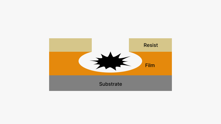
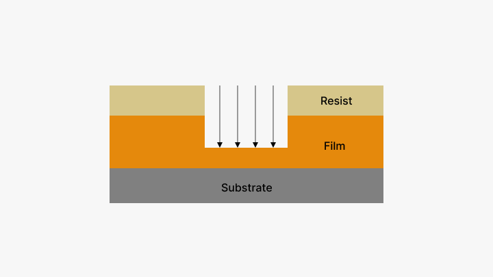
Photochemical Etching
Photochemical etching involves the photochemical process by which a light-sensitive photochemical resist is applied on the substrate of a PCB. That resist is then exposed to UV light through a patterned mask. The unexposed areas are washed out, and the exposed areas are then chemically etched. This process makes it realize very good accuracy and is mainly applied for complicated circuits.
Dry Film Resist Etching:
A photosensitive dry film resist is laminated onto the copper surface, exposed to UV light, and then developed to remove the uncured resist. This gives very accurate selective etching.
Liquid Photoresist Etching:
Coating with liquid photoresist and curing by UV radiation, after which it is dissolved selectively with a solvent in order to increase control in the course of the etching process.
Electroless Copper Deposition
This includes overlaying a thin layer of copper on the entire surface of the PCB to make it more conductive and prevent the circuit traces from oxidizing. Among many others, this is seen as improving overall performance and reliability in PCBs.
Advantages and Disadvantages of Etching Techniques
Wet Etching
Advantages
Fine surface uniformity.
Generally, wet etching is appropriate for nearly all metals, glass, and plastics.
A relatively cheap process, especially for large quantity production.
Great selectivity where only the intended material undergoes etching.
Disadvantages
Isotropic etching can result in undercutting.
Pattern fidelity may be less accurate.
The control of the smallest line features is difficult to obtain.
Dry Etching
Advantages
Anisotropic etching with good control over the etching profiles.
Photoresist shedding is very minimal, hence more reliable.
Etching uniformity is excellent.
Chemical costs are reduced as well as environmental impact.
Disadvantages
Limited etching options for the underlying material.
Plasma-induced damage may occur.
Equipment is expensive.
Best Practices in PCB Etching
The following are best practices in etching PCBs for the best results:
Agitation of the Etchant
Effective agitation of the etchant would maintain consistency in the etching rate and avoid disparities in traces. One should stir or agitate the etchant from time to time during the process.
Temperature Control
The temperature of the etchant should be just right to avoid over-etching and traces that are not up to the mark. Higher temperatures hasten the process but need due diligence in managing it.
Masking and Alignment
Alignment should be accurate, with appropriate masking techniques. Employment of high-quality masks and ensuring alignment accuracy will lead to the correct pattern in the circuit.
Conclusion
The capability to etch PCBs is one of the most valuable processes within the making of printed circuit boards in achieving such ramifications of circuitry intricate enough to control modern electronic devices. By focusing on best practices and understanding traditional and innovative techniques for etching, manufacturers can fabricate high-quality PCBs that attain higher performance and reliability. With continuous improvements in technology, embracing new methods and innovations in PCB etching will play a key role in meeting the ever-growing demands within the electronics industry.
It's an even deeper appreciation from within the realm of etching on printed circuit boards, due to the precision and expertise it takes to create this small piece of the electronic circuit powering our devices. The future in store for the manufacture of printed circuit boards holds exciting possibilities for the innovation and improvement that has been made using traditional methods of chemicals up to very advanced methodologies.
Hot Tags:

Contact us

If you can't find what you're looking for, please contact us.
Article
The silkscreen layer, made of non-conductive ink, is vital for identifying PCB components and ensuring accurate placement. Methods like Liquid Photo Imaging and Direct Legend Print enhance precision. PCBX excels in producing high-quality silkscreen applications, crucial for proper assembly and functionality.
 2024/08/21
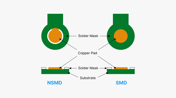
Solder masks protect PCBs from environmental damage and electrical shorts, enhancing reliability and aesthetics. The application is complex, requiring professional fabrication to ensure quality and compliance with regulations.
2024/08/20
Backdrill in PCBs removes stubs in vias to improve signal integrity and impedance control, crucial for high-frequency, multilayer boards. It’s vital in communication, servers, medical, and aerospace applications.
2024/08/01