PCB Insertion Loss
PCB insertion loss is crucial to managing signal attenuation in high-frequency designs, affected by materials, path length, and connectors—optimized through strategic design measures.
In the complex world of PCB design and engineering, there are many challenges. Among the biggest concerns for an engineer is how to handle insertion loss, the loss of signal strength through traveling via circuits and interconnections. While there are some types of losses, such as those associated with thermal management, that are intentional, insertion loss generally represents unwanted attenuation that can degrade system performance, particularly in high-frequency applications. The focus of the article is thus on the elucidation of various intricacies related to PCB insertion loss, highlighting their key contributors and showing ways in which their after-effects can effectively be minimized.
Insertion loss is one of the critical performance parameters that quantify the amount of signal power reduction while negotiating the PCB and its associated system components. Conventionally measured in decibels, it shows the attenuation encountered by the signal while flowing across the circuit paths and is commonly present in high-speed electronic applications operating above 3GHz frequencies. It is representative of the cumulative amount of energy loss including conductive, dielectric, radiation, and reflective losses within a given path of the circuit.
Key Contributors to Insertion Loss
The mitigation of insertion loss can only be effective if the root causes are understood. The main factors contributing to insertion loss in PCB systems include:
Transmission Length: The path length of a transmission is proportional to the extent of signal attenuation. Longer transmission paths introduce increased resistance, raising conductive loss, but are also more difficult to impedance-match. Longer transmissions are also easier to interfere with and inductively couple.
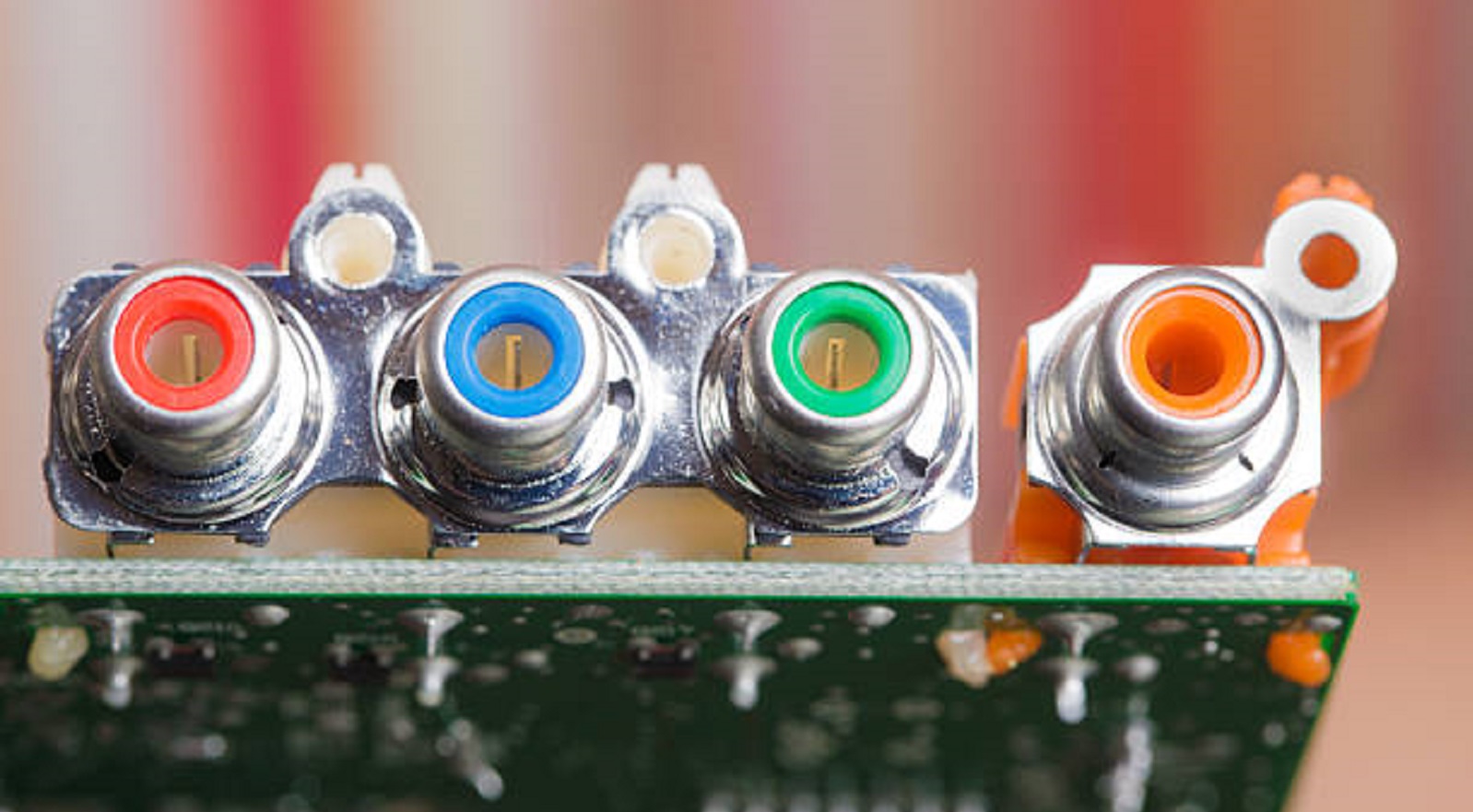
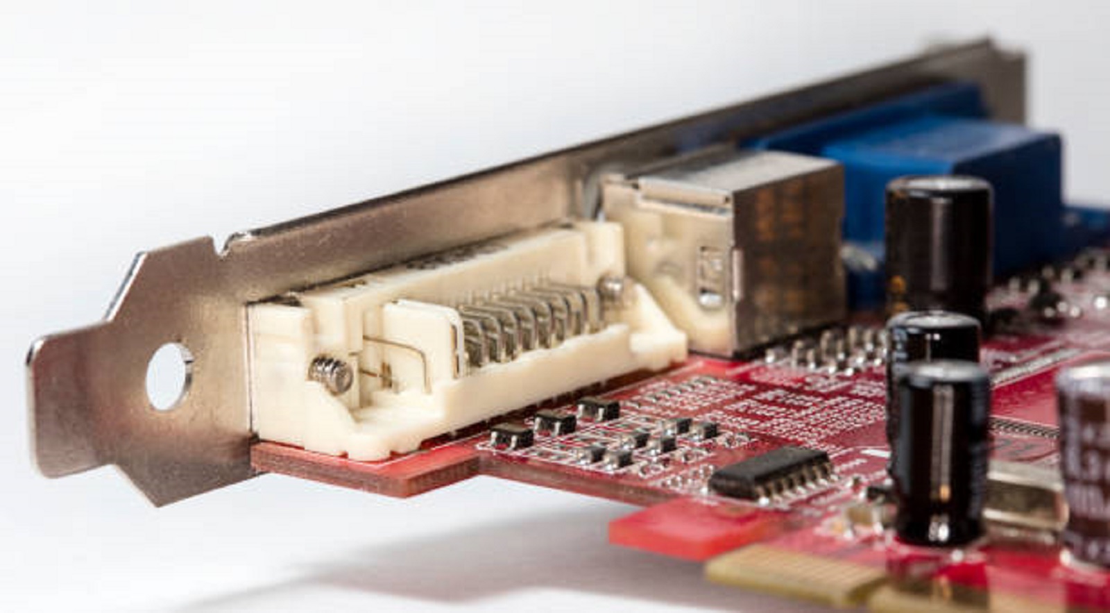
Connectors and Cables: Interconnects comprise the majority of a system's overall insertion loss. The connectors can provide impedance discontinuities that reflect signals, result in phase distortion, and return loss. These reflections are further amplified by connectors and terminations, which can decrease the VSWR at the system stage. In many cases, the physical characteristics of connectors-the pins and associated pads-have been sources of inductive and capacitive impedance discontinuities.
Material Characteristics: The dielectric and conductive materials in the composition of PCBs contribute to insertion loss. Materials with high dielectric constants and loss tangents are seen to dissipate more power in the transiting signal. Copper thickness and smoothness, combined with the type of dielectric material used, have a telling effect on the degree of both conductive and dielectric losses.
High-frequency Effects: Above 10GHz, many other factors such as the skin effect start to become more influential. The skin effect is one wherein the signal current flows through the surface of the conductor; hence, it increases resistance, which in turn increases the insertion loss. This effect shows that understanding how frequency-specific behaviors affect the overall performance of the system is crucial.
Strategies for Mitigating Insertion Loss
Several strategic measures can be taken by a PCB designer and engineer to counteract insertion loss:
Optimize Transmission Paths: The practical lengths of transmission should be as short as possible. This minimizes resistance and hence potential interference. In natural courses, shorter paths have reduced inductive and capacitive losses.
Select Appropriate Connectors and Cables: Which do not introduce impedance discontinuities or improve VSWR. Newer solutions, such as UPC, have inherently lower insertion loss and are suitable for high-speed applications.
Use Low-loss Materials: The low dielectric constant material and smooth copper finish are the two crucial ingredients that constitute a PCB stack-up. Both the dielectric and conductive losses will be reduced by these factors. Additionally, laminate thickness is checked with the operational frequency that is expected.
Consider High-Frequency Design Implications: At higher frequencies, the main focus should shift toward skin-effect reduction and should be taken into consideration during PCB construction. Smaller-sized conductors, designed stack-up geometry can reduce the impact of all such issues.
Advanced Simulation and Modeling: Modern electromagnetic simulation tools give great insight into possible insertion loss challenges at the design phase. By modeling transmission lines and component interactions, designers can anticipate issues and make necessary design modifications before production.
Balancing Performance and Cost
While these above strategies will go a long way in reducing insertion loss, most of them come with their own set of trade-offs, mainly regarding production cost. High-performance materials and special components may inflate the cost of manufacture. Consulting experienced PCB fabrication and assembly providers can help designers make these trade-offs. These partners possess operational know-how and advanced technologies for design optimization to achieve the right balance between cost efficiency and signal integrity.
The insertion loss is one of the major challenges in the design of high-speed PCBs. A deep understanding of its causes and effects, together with strategic design and material selection by an engineer, can reduce its impact. This will be in cooperation with industry experts-for instance, PCB fabrication and assembly specialists. Such collaboration will make sure that the several trade-offs accompanying high-performance design are duly managed for optimized electronic systems capable of maintaining robust signal integrity in these so-called demanding applications. With the consistent soar in frequency demands for modern electronics, insertion loss will continue to be very key and will have to be addressed with precision and foresight in the pursuit of excellence in PCB design.
Hot Tags:
Contact us

If you can't find what you're looking for, please contact us.
Article
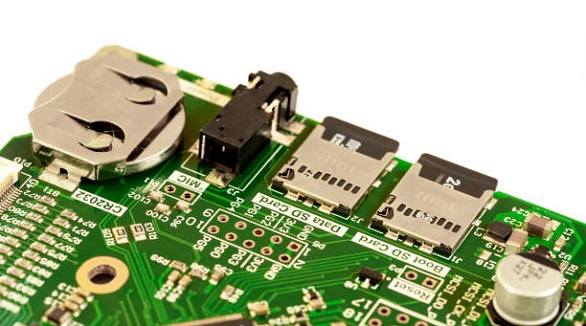
PCB edge mounting optimizes space, enhances modularity, and improves connectivity by placing connectors on board edges, aiding in flexible, efficient system design.
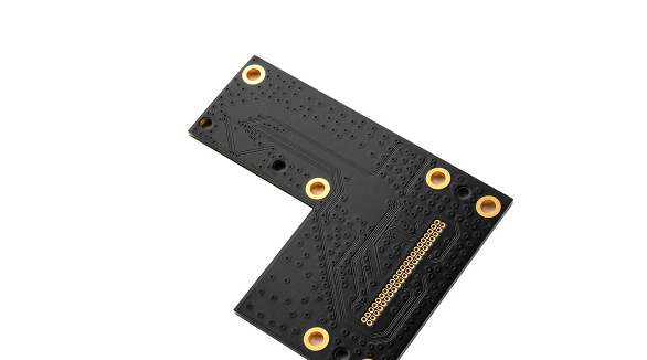
Plated-through slots (PTS) in PCBs are copper-plated apertures for electrical connectivity, offering space optimization, reduced soldering voids, and improved surface use.
Backdrill in PCBs removes stubs in vias to improve signal integrity and impedance control, crucial for high-frequency, multilayer boards. It’s vital in communication, servers, medical, and aerospace applications.