- Products & Capabilities

- About
- Resources
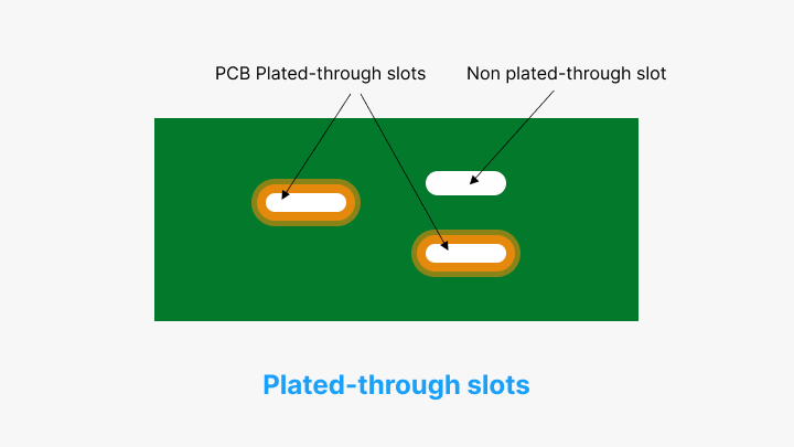
PCB Plated-Through Slots


Plated-through slots (PTS) in PCBs are copper-plated apertures for electrical connectivity, offering space optimization, reduced soldering voids, and improved surface use.
Plated-through slots refer to the holes in a printed circuit board, electroplated with some kind of conducting material to permit the establishment of electrical connection across the layers of a PCB. In this article, the essence of PTS will be discussed from four aspects: definition, advantages, design considerations, and the manufacturing process.
Definition
Plated-through slots are copper-plated apertures designed for electrical connectivity, serving as a means of executing through-hole plating on PCBs. The slots are contrasted with edge plating, which happens at the periphery of the PCB. These slots may be classified into plated through holes or non-plated through holes. A plated through hole is made where there is a top and bottom connection between milling and copper. These slots can accommodate through-hole device pins and can be done, on a PCB, in both plated and non-plated configurations.
Advantages
Plated-through slots have several advantages, especially for rectangular-pinned components. They offer a much more efficient use of space compared to standard round holes, which often waste a lot of space. The primary advantages include:
- Space Optimization: Reduces the gaps between the component pins and the PCB to facilitate compact and efficient design.
- Soldering Advantages: Reduces soldering voids, since slots accommodate big rectangular leads nicely without any extra gaps once the leads are placed.
- Space Maximization on the Surface: Allows for the exact setting of the lead slots, which may make more space available on the surface of the PCB.
Design Consideration
For a plated-through slot, the length and width of each slot have to be well-defined at design to ensure clarity of the manufacturing drawings about the production requirements. In the EDA tools, one may define plated through slots using elliptical holes or in the Gerber mechanical layer. If no mechanical layer is defined in the design file, add a mechanical layer, and place the slot definition therein. It's also good to add a README document to this directory which documents the PTS requirements.
Manufacturing Process
PCBX provides a minimum width of 0.5mm for plated-through slots and 0.8mm for non-plated-through slots. The first involves milling processes to erode the respective slot width from the PCB material, removing excess copper to create solder pads, traces, and other requirements. Thereafter, relevant drilling techniques are used to drill the slots as per requirement based on design specifications. This is followed by the removal of residues after cleaning, and then the slots are immersed in copper chemical plating similar to through-hole plating. Final surface treatments complete the process. For devices having rectangular or unusual shape pins, round through-holes can result in excessive voids. Therefore, the best design practice is to provide slots for the exact pin shape to fit the pins.
Hot Tags:
Contact us

If you can't find what you're looking for, please contact us.
 2024/07/29