- Products & Capabilities

- About
- Resources
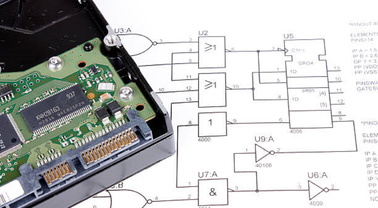
PCB Schematic vs. PCB Layout


PCB schematics map circuit connections, while layouts focus on physical design for manufacturing. Both stages ensure optimal and reliable PCB design.
Precision and strategic planning are key in the very fast pace that defines the world of electronics design for the success of any project. Schematic design and layout design are two critical phases in the development of printed circuit boards. While both these stages are important and interconnected, they play different roles. Using my expertise from the field, this paper leverages work experience from the industry leader PCBX and details below the principal differences between schematic and layout as regards the general aspects and functionality associated with producing workable electronics.
What is a PCB Schematic?
The PCB schematic diagram is a two-dimensional representation of the relationships and interactions between the electrical components on a circuit board. The circuit's conceptual map is used to identify the electrically related resistors, capacitors, and integrated circuits. Its main goal is to describe the logically continuous signal paths, without considering rail routing or the location of physical components.

Essential Components of a PCB Diagram:
Component Symbols: Standard representations are provided for the symbols of various components on the schematic diagram. The representation of a symbol is important, for clarity, and to allow communication among all the different players.
Definition of the Signal Path: The schematic shall have logically organized signal paths laid out to convey how each of the components relates in the said circuit. This may show specifically how the anode of one diode links to a certain transistor pin.
Validation of Design: Simulation of a schematic will let the designers validate the expected behaviour of the circuit before the real layout. One can debug, troubleshoot the problems, or optimize in that virtual environment only.
Recording: Schematic schematics give the essential documentation that engineers, technicians, and other teams follow to maintain knowledge and implementation harmony.
What is a PCB Layout?
The schematic varies from the layout in that the circuit design now adopts a practical format for production, component placement on the board, and the path drawing for determining the connections between these discrete components. During this stage, a variety of physical restrictions related to manufacturing feasibility and performance optimization must also be followed, along with very stringent design specifications.
Component arrangement: A smart layout design includes the careful arrangement of components to maximize space, minimize interference, and efficiently control thermal effects.
Trace Routing: This is designing the copper paths that connect the components, taking care of electrical performance, trying to avoid interference, and keeping in line with design specifications.
Layer Management: Modern PCBs use multiple layers due to complex circuits. The engineers are supposed to arrange the signal, ground, and power planes carefully.
Design Rule Compliance: The layout is done according to particular design rules concerning trace width, spacing, and pad size for manufacturability and the reliability of the board.
Thermal Management: Engineers may keep the operating components within a safe temperature range, enhancing device performance and extending life, by accounting for heat dissipation during layout design.
How PCB Layout and Schematic Differ
Despite being equally important stages in the design cycle of a PCB, they are managed differently and have distinct traits:
The following describes the nature of the representation: A schematic is a two-dimensional design that looks at electrical interconnection, whereas a layout is a virtual three-dimensional representation that concentrates on physical execution and manufacturing viability.
Project Process: For conceptualization purposes, schematics are a fundamental drawing that must be completed before the layout in any design job. A missing schematic gives no information about location or route.
Handling Signal Paths: Without being constrained by physical limitations, the signal lines in a schematic cross one another to provide logical communication. However, in layout design, the crossing of physical traces is avoided to a great extent; this is mostly managed through multiple layers to avoid interference between signals.
Complexity Management: Schematics might use multiple pages or blocks to divide complex circuits into more comprehensible pieces; layouts manage complexity by using strategically arranged layers and routed traces.
Importance in Electronics Design
The knowledge of both schematic and layout stages is very important in the development of an electronic product.
Error Minimization and Performance Optimization: This is where a complete and validated schematic minimizes potential errors early in the process, while an optimized layout ensures electrical performance and signal integrity.
Manufacturability and Cost Efficiency: Well-designed layouts, following manufacturing guidelines, can save money by avoiding costly rework and staying within production capabilities.
Scalability: A good schematic and layout mean designs can be scaled up to more complex systems or adapted and improved upon in existing designs.
Effects of PCB Layout on Current Return Path and Signal Integrity
It forms the basis on which signal paths are defined and current behavior controlled, hence determines the overall performance of the signals and the boards. Good management of layers, trace routing, and strategic placing of components ensures control of return signal paths to minimize electromagnetic interference. These are parameters which a designer must consider while making a design for robust high-frequency PCBs.
In the design of a PCB, the schematic and layout stages are interrelated elements when it comes to constructing reliable electronic devices. The schematic captures an abstract relationship that describes how components logically interact with each other. On the other hand, layout presents these ideas in a manufacturable format. Expertise in both stages is necessary for making sure that functionality and reliability are maintained in the final product. At PCBX, we avail you of experience and solutions with which to usher you through those critical stages accurately and efficiently for the realization of your designs. Whether it is a new project or refining, our commitment at every step guides you through to excellence in your electronic design.
Hot Tags:

Contact us

If you can't find what you're looking for, please contact us.
Article
Effective management of load current in PCBs ensures reliability and safety, essential for modern technology across sectors like communications and medical devices.
 2025/01/20
Edge connector bevelling enhances PCB durability and reliable connections, vital for frequent usage and secure engagements, with limitations primarily in plating.
2024/12/25
Solder masks protect PCBs, while paste masks aid precise component placement during assembly, both crucial for PCB reliability and efficiency in electronics.
2024/10/28