- Products & Capabilities

- About
- Resources
PCB Side Plating


PCB side plating, or edge plating, involves copper along PCB edges, enhancing connectivity, conductivity, shock protection, and assembly, especially for small boards. Used in Wi-Fi and Bluetooth modules, it improves signal quality and EMC. Limitations include necessary design gaps and exclusion of V-cuts.
What is PCB Side Plating?
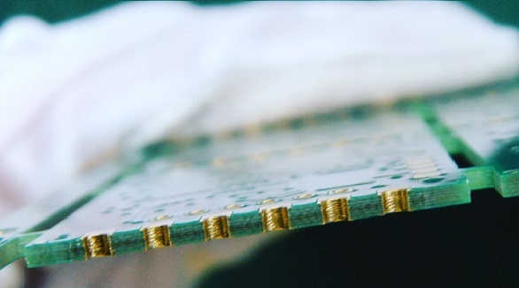
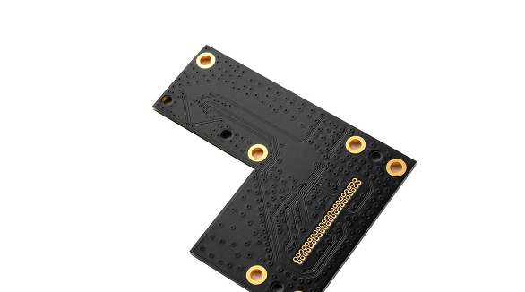
PCB side plating, also known as edge plating or castellation, is a copper plating that runs from a PCB's top to bottom surfaces and along at least one of its perimeter edges, which ensures fine connectivity through the board while reducing the risk of failures in equipment, mostly the small form factor boards and sub-motherboards. Common implementations can be found in Wi-Fi and bluetooth modules.
During fabrication, the metallization outer edges are milled before starting the copper plating process. Once the copper has been deposited, a suitable surface finish, typically ENIG—Electroless Nickel Immersion Gold—is added to the PCB's edges.
When is Circuit Board Side Plating Used?
Edge plating is used in several instances, including:
- Improved Conductivity: To improve conductivity in general.
- Edge Connection: When connections are needed across the edge of the PCB.
- Shock Protection: To protect the board from lateral shocks.
- Secondary Connections: When secondary circuit boards are linked to a mainboard using edge connections.
- Improved Assembly: For improved soldering at the edges.
Design Parameters for Edge Plating
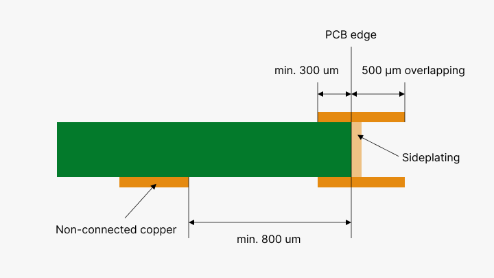
The metalized area for edge plating is defined by overlapping copper, either on the surface, pads, or tracks in a CAD layout. Specific design parameters include:
Overlap: The overlap must be at least 500 μm.
Connected Layers: Specify at least 300 μm of connected copper.
Non-connected Layers: Ensure there is a minimum of an 800 μm gap from the outer contour.
Side Plating Benefits
- Signal Quality in High-frequency Boards: Enhances signal integrity, which is crucial for high-performance circuits.
- Electromagnetic Compatibility (EMC): Helps enhance EMC in multilayer PCBs.
- Shielding: Inner layer shielding becomes an important application where external interference on the signals gets reduced.
- Electrostatic Protection: Aids in preventing electrostatic damage during transportation.
Limitations
- Gaps Required: The whole edge cannot be plated in one piece due to the necessity of retaining the PCB in the production panel—gaps must be included when placing the routing label.
- Excluded Processes: V-cutting scores cannot be used on plating that requires edge plating because a layout must be provided before performing the through-hole plating process.
Conclusion
Immersion gold or silver finishes are recommended for flawless edge plating. Apart from that, in the case of the solder mask layer, create an opening in the solder mask file and use textual annotations to express specific requirements. Side plating improves the performance, reliability, and longevity of PCBs by adhering to the principles and design factors listed above.
Hot Tags:
Contact us

If you can't find what you're looking for, please contact us.
 2024/07/29