- Products & Capabilities

- About
- Resources
PCB Silkscreen


The silkscreen layer, made of non-conductive ink, is vital for identifying PCB components and ensuring accurate placement. Methods like Liquid Photo Imaging and Direct Legend Print enhance precision. PCBX excels in producing high-quality silkscreen applications, crucial for proper assembly and functionality.
While designing or ordering a printed circuit board, have you wondered if the silkscreen layer was really necessary, and if so, at what extra cost? Let's see what a silkscreen is and why it's important in PCB manufacturing.
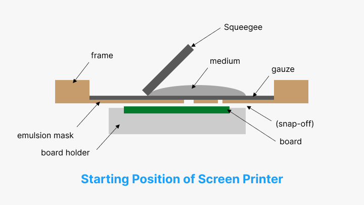
What is Silkscreen?
Applied on the PCB for identification purposes is the silkscreen, otherwise known as the layer of non-conductive ink: components, test points, parts, warning symbols, logos, and other markings. Normally, this should be applied to the component side, but sometimes this is placed on the solder side of the board. A more detailed silkscreen will help the manufacturer and the engineer locate where all the components of a PCB will be placed.
This layer uses epoxy ink, normally black, white, or yellow, and most PCB software uses standard fonts for these markings. Conventionally, silk-screening would require the following tools: a polyester screen stretched on aluminum frames, a laser photo plotter, a spray developer, and curing ovens.
The silkscreen layer can include important information, such as:
- Polarities of parts
- Location of parts through reference designators
- Test points
- Unique identification numbers for each board
- Warning symbols.
The Importance of Silkscreen in PCB Assembly
In the past few years, silkscreen applications have undergone a shift from the use of stencils to direct application methods. Currently, there exist two major methods which are applied in the printing of silkscreen on a PCB. These are liquid photo imaging and direct legend print.
- Liquid Photo Imaging (LPI): Using line widths greater than 4 mil, liquid photo-imageable epoxy is coated onto the laminate and exposed with UV light, then developed and cured on the board, providing increased accuracy compared to manual screening.
- Direct Legend Printing (DLP): This offers the highest accuracy at a higher cost. The inkjet projector sprays acrylic ink onto the raw PCB guided by CAD data, and UV light cures the ink as it comes out from the printer. Note that acrylic ink does not cure well on boards finished with silver.
While silkscreen application happens during fabrication, it is extremely important for assembly, which involves component placement or mounting. Some key silkscreen markings that facilitate proper placement include:
- Reference Indicators: Explains what kind of components are from the BOM.
- Pin 1 Indicators: Shows which pins connect to what pads of the footprint.
- Component Outlines: Combined with the landing pattern, these indicate where the components should be placed.
- Polarity Indicators: Indicate the orientation of polarized components.
For parts with few pads or simple shapes, omission of the component outline for general placement may be acceptable. It will then create asymmetrical placement issues, such as tombstoning, in soldering. The absence of reference, Pin 1, and polarity indicators can make a component be oriented or placed incorrectly. This would then lead to poor device functionality.
PCBX's expertise in silkscreen
PCBX has become one of the most experienced manufacturers for PCBs and PCB assembly in China, having been an industry leader for almost two decades. PCBX specializes in quick-turn PCB prototypes and assembly, as well as medium and small volume PCB manufacturing, and strives to satisfy all of your silkscreen requirements with high quality and precision on every project. Cooperating with PCBX will provide you access to our expertise and dedication to superior silkscreen application on your PCBs.
Hot Tags:

Contact us

If you can't find what you're looking for, please contact us.
Article
PCB side plating, or edge plating, involves copper along PCB edges, enhancing connectivity, conductivity, shock protection, and assembly, especially for small boards. Used in Wi-Fi and Bluetooth modules, it improves signal quality and EMC. Limitations include necessary design gaps and exclusion of V-cuts.
 2024/08/21
Selecting the right PCB surface finish, from options like HASL, ENIG, ENEPIG, and OSP, is crucial for preventing oxidation, ensuring solderability, and meeting reliability standards.
2024/08/07
PCBs (Printed Circuit Boards) are fundamental in electronics, composed of multiple layers like silkscreen, soldermask, copper, and substrate, chosen for specific electrical functions.
2024/08/07