PCB Simulation
PCB simulation enhances design precision and efficiency by predicting behavior, reducing errors, and optimizing performance before prototyping, thus saving costs and time.
In the fast-moving world of electronics engineering, designs and developments related to printed circuit boards are at the forefront of requiring high precision and efficiency. The designers are expected to create systems that meet exacting specifications, ensuring further reliability and performance. Engineers use an ever-increasing dependence on the simulation of PCBs as a strong tool in the virtual testing and validation of board designs before their physical prototypes are made. This article will go into the details of how PCB simulation works, its benefits, methodologies, and how it is a must-have in the advancement of electronic design.
PCB simulation is done using software packages to model and analyze the behavior of an electronic circuit board. By the use of simulation, an engineer can determine how the PCB will behave under a number of real conditions by highlighting problems that may exist in the design and giving recommendations for the improvement of such functionalities. This decreases the likelihood of costly mistakes and shortens development durations.
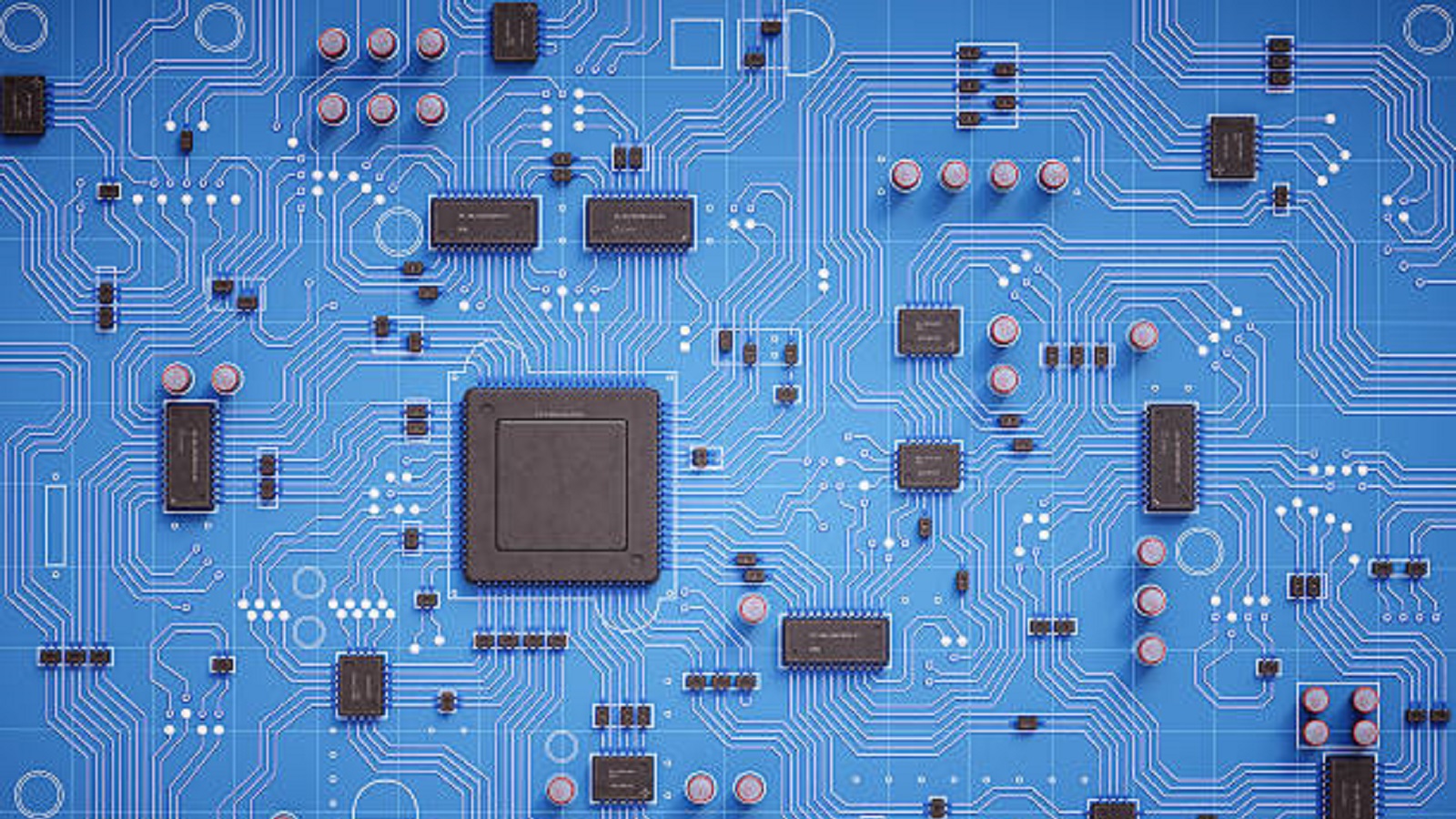
Simulation software supports a wide range of analysis, including:
Signal Integrity Analysis: As electrical signals pass across the PCB, their quality is assessed. It aids in the detection of problems like as reflection, crosstalk, and signal attenuation, all of which can decrease performance in high-speed devices.
Thermal Analysis: This predicts the heat distribution and hotspots on a PCB. This analysis is critical because it helps ensure components will operate within safe temperature ranges, extending their life span and preventing failures.
Power Integrity Analysis: It analyzes how power is distributed within the PCB and ensures stable voltage levels all over the board. It is important to prevent power-related issues that might compromise dependability and functionality.
Electromagnetic Compatibility (EMC) Analysis: This guarantees that a printed circuit board won't generate electromagnetic interference or be vulnerable to it. To ensure that the PCB won't interact with other devices and to comply with regulatory norms, this examination is crucial.
Benefits of PCB Simulation
The integration of simulation in the design process has a number of advantages:
Cost Efficiency: Simulation reduces the need for multiple prototypes, saving a lot of money by finding errors in the design phase through virtual testing.
Time-Saving: Simulation speeds up the design cycle since designers can make fast changes in response to analysis results, hence optimizing designs before fabrication.
Improved Design Quality: Through comprehensive analysis, simulations ensure high-performance designs that meet specifications, thereby reducing the risk of field failures and returns.
Risk Mitigation: Detailed simulations can foresee operational issues that make sure the designs are robust enough to bear most real-world challenges.
Enhanced Innovation: Engineers can explore different design approaches and alternatives virtually, fostering innovation without the constraints imposed by traditional prototyping.
Methodologies in PCB Simulation
The PCB simulation uses various methodologies for performing analysis in several fields of board design, as described below:
FEA: Thermal and Mechanical Analysis: The FEA splits a PCB into a network of small finite elements for correct analyses such as stress, temperature, among others.
Circuit Simulation: It gives a simulated environment in which to evaluate how circuits function. SPICE (modeling Program with Integrated Circuit Emphasis) allows for the modeling of analog circuit performance, component selection, and optimization.
Field Solvers: These instruments compute the electromagnetic field distributions over the printed circuit board (PCB), which are critical for signal integrity and EMC investigation. They give exact information about how design changes affect electromagnetic behavior.
PCBX Simulation Tool
PCBX meets and exceeds the complexities being thrown upon today's electronic engineering, including various functionalities that shall ease the effort spent on simulating the said board, including the following:
User-Friendly Interface: Allows a user in the software to efficiently go through creating and conducting the simulation in the easiest of fashions.
Comprehensive Suite of Analysis: Offering a wide range of analyses to ensure that all aspects of a PCB's performance are optimized.
High-Performance Computing: By employing powerful computing powers, PCBX effectively shortens the time required for each design iteration by delivering trustworthy results rapidly.
Integration in the Design Process
The steps involved in the incorporation of simulations in the PCB design are listed below.
Initial Design: A layout of the printed circuit board along with the schematic has to be prepared with the aid of CAD tools.
Set Up Simulations: Identify the simulation parameters and constraints according to design requirements and expected use cases.
Run Analyses: Perform comprehensive analyses regarding signal integrity, thermal performance, power integrity, and EMC.
Iterate and Optimize: Inform the modifications using the results from the simulations, iterating through refinement as needed.
Verification: Once the performance has been confirmed through simulation, go ahead with the prototype and testing in the real world.
Challenges and Prospects
PCB simulation offers advantages, but it also has disadvantages. Detailed component libraries and often complex setup processes are required to ensure realistic models. In addition, the computational needs of simulations may necessitate a significant amount of time and processing capacity for detailed analysis. In the future, simulation software developments will continue to enhance usability and accuracy.
The reason is that PCB simulation provides designers with a virtual workshop where they can perfect their idea before investing in prototypes. Further advances in the capabilities of technology will extend the capabilities for simulation in tools, leading to designers' abilities in creating ever more sophisticated, yet increasingly reliable, electronic systems. Incorporating simulation at the forefront of the process not only makes it better but allows new opportunities in innovation and perfection for electronic designs.
Hot Tags:
Contact us

If you can't find what you're looking for, please contact us.
Article
Tab routing in PCB manufacturing boosts efficiency and quality, ideal for non-linear shapes, offering flexibility, support, and cost-effectiveness in production.
PCBX's new platform streamlines PCB design, offering real-time simulations, prototyping, and collaboration tools for students, hobbyists, and professionals.
Mixed Assembly PCBs combine Surface Mount Technology (SMT) and Through-Hole Technology (THT) for high-performance, compact, and reliable circuit boards. This integration leverages both technologies to enhance reliability, component selection, flexibility, and efficiency. Used in CPUs, IoT hardware, and more, they offer economic, efficient manufacturing for versatile applications in modern electronics.