- Products & Capabilities

- About
- Resources
PCB Solder Mask and Design Tips


Solder masks protect PCBs from environmental damage and electrical shorts, enhancing reliability and aesthetics. The application is complex, requiring professional fabrication to ensure quality and compliance with regulations.
After the etching process, the air directly meets the copper wires on the PCB substrate. Pollution like dust and dirt, upon falling on the circuit board, is most likely to defect it by initiating electrical shorts on the PCB. In addition, since copper is a metal and due to its reactivity, it reacts chemically with air. These reactions can degrade its conductivity and ultimately shorten the lifespan of the PCB. Hence, the application of a protective film, known as a solder mask, becomes a critical step in the manufacturing process.
Definition
A solder mask is a thin protective layer applied over copper traces of a PCB, sometimes also called a solder resist or a solder-stop mask or coating. It covers areas where there is no need for soldering on either the top or bottom sides, ensuring high performance and reliability in the PCB. The resin is usually chosen as the main material of the solder mask because it provides all the properties related to proper resistance to humidity, insulation, resistance to solder, resistance to high temperature, as well as the properties related to design aesthetics.
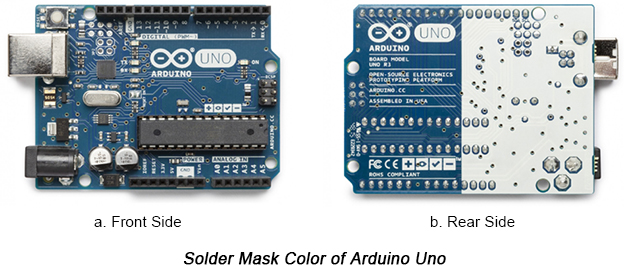
It is well known that most PCBs are green; this color is the color of the solder mask green oil. However, solder masks are available in various colors like white, blue, black, red, yellow, and so on. The choice of the colors depends on the specific requirements. For instance, some R&D teams might opt to have prototypes with a red solder mask made in the NPI stage so that they can easily be distinguished from the rest of the lot. A black solder mask may be needed to match the color of enclosures in a final product where boards are partially (or fully) exposed.
Interestingly, two different sides of a PCB can have solder masks with different colors. For example, the following is an Arduino Uno board:
Functions
Due to the rising density of boards and SMT now being the solution of choice due to market demands for volume and efficiencies, solder masks have become extremely popular and vital for circuit boards.
As the name implies, the primary function of the solder mask is to prevent solder bridges from occurring on the covered areas. One of the most important aspects of SMT assembly is reflow soldering. These are responsible for ensuring that electronic components are mounted correctly with the solder paste on the circuit boards, and the main functions are as below.
Environmental Protection: The solder mask prevents the entry of dust, moisture, chemicals, and other impurities which may corrode or damage the copper traces besides other parts of the PCB.
Solder Bridges: Molten solder may flow from one pad to the neighboring one, thus forming a solder bridge across neighboring pads, resulting in a short circuit. The solder mask prevents this by covering the areas that should remain free of solder.
Increased Reliability: The solder mask also adds overall reliability and durability to the PCB, as it will protect copper traces and other sensitive components from oxidation and potential contamination.
Aesthetic and Functional Identification: While PCBs are basically identified by their green color, alternative colors may be red, blue, black, and white, which are applied by the solder mask. This is useful during the assembly and maintenance by visually examining the circuit routes and the components.
Electrical Insulation: A layer adheres to exposed copper so that it's only present at points where components need to be soldered.
Manufacturing Process
Many engineers believe that manufacturing a solder mask is not so much technically difficult and it's possible to do it at home, however, that's quite wrong. Although the DIY solder masking may work with some simply designed boards, ensuring its reliability in a project's final product is complexly possible unless the solder mask is applied professionally.
Now, for professional PCB fabricators, solder mask manufacturing is in no way straightforward. It requires thorough compliance with a multitude of stringent regulations like ISO9001, UL, or RoHS. The process consists of different stages, each having a high accuracy that is derived from mature technologies, extensive experience in manufacturing, and up-to-date equipment at their disposal.
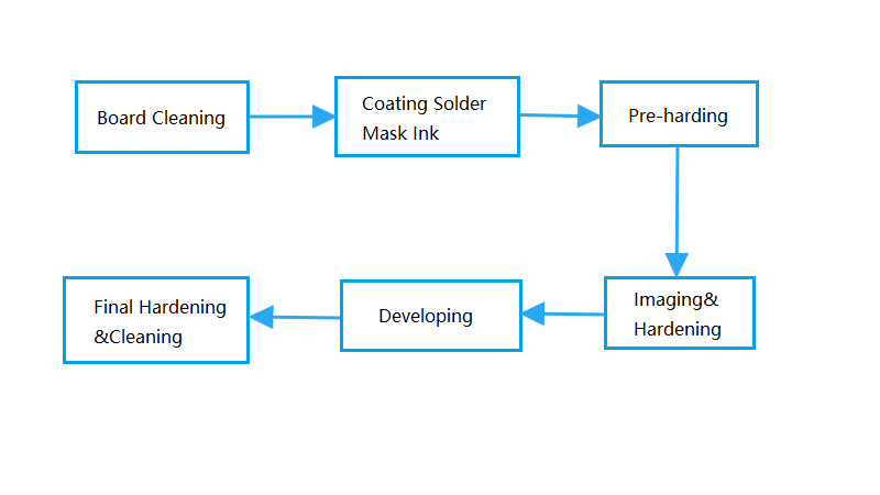
Step 1: Board Cleaning
This step aims at cleaning the board's surface from tarnish or dirt and keeping it dry.
Step 2: Coating Solder Mask Ink
The cleaned board is then loaded into a vertical coater for the coating of solder mask ink. The thickness for coating will depend on several factors, including the circuit boards' reliability requirements, the fields they serve, and the thickness of the board itself. The board surface is not as flat as one might consider, and coating thickness may vary across different areas of the board, such as traces, substrate, or copper foil. Experienced PCB manufacturers call out specific coating thicknesses based on equipment capability and manufacturing experience.
Step 3: Pre-hardening
This is done to make the coating relatively solid on the board so that extra coating will come off easily at the developing stage.
Step 4: Imaging and Hardening
Mount the transparent film with circuit images on the board and expose it to UV. The solder mask, covered by the transparent parts of this film, is hardened by the exposure, but the pre-hardening state remains on the part with the circuit image. During hardening processes, proper alignment should be ensured to avoid copper foil exposure in non-designated areas, which may cause short circuits or destroy the performance of the circuit board.
Step 5: Developing
The PCB is dipped in a developer to remove the unwanted solder mask and make the copper foil, which is supposed to be exposed, correctly exposed to it.
Step 6: Final Hardening and Cleaning
Final hardening ensures that the solder mask ink is thoroughly dried on the surface of the PCB. Then the boards are cleaned before surface finishing and assembly processes are carried out.
Design Tips
No matter which PCB design software is used, it is not necessary to design a solder mask, which is easily designed after filling in some parameters, and some software can even support automatic solder mask design.
This will be critical before actual designing is initiated, as one has to consult with the contracted PCB manufacturer for their capability regarding solder mask thickness and the minimum spacing between copper pads.
Small problems with the solder mask, such as too little solder mask opening or too much, and mismatches between the number of openings and copper pads in the circuit plane, can cause circuit board failure. This may be due to carelessness or modification of the design files; it takes a long time to confirm. Some problems may even result in severe damage. That is why your design files should be reviewed.
Choose PCBX to Help Solder Mask Design
With over 20-year hands-on expertise in the electronics industry, PCBX is well-equipped to provide solder mask color and design recommendations/consultation solutions. Please contact us if you have any PCB design questions.
Hot Tags:

Contact us

If you can't find what you're looking for, please contact us.
Article
Ensuring BGA soldering quality involves defect prevention, pre-soldering measures, and precise control during SMT assembly and reflow soldering.
 2024/08/20
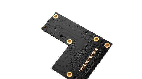
Plated-through slots (PTS) in PCBs are copper-plated apertures for electrical connectivity, offering space optimization, reduced soldering voids, and improved surface use.
2024/08/06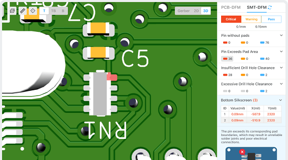
The article is developed concerning the breakthrough of integrated circuits and the need for custom PCBs in some electronic products. It enumerates ten golden rules in conducting PCB layout design and manufacturing: grid selection, routing, power layers, component placement, panel duplication, component value combination, frequent DRC, flexible silkscreen use, decoupling capacitors, and pre-production parameter checks. These rules provide for the optimum design and manufacturing of a PCB.
2024/07/25